Chinese Chipmaker SMIC Orders $120m EUV System
Semiconductor Manufacturing International Co. (SMIC), China's top state-backed contract chipmaker, has reportedly ordered a set of extreme-ultraviolet lithography equipment from Dutch ASML.
SMIC's reserved EUV system is expected to be delivered by early 2019, according to Nikkei Asian Review.
The move highlights its growing ambition to help boost Chinese homegrown semiconductor manufacturing technology, even though it is still two to three generations behind market leaders.
All top global chip giants, including Intel, Samsung Electronics and Taiwan Semiconductor Manufacturing Co. are buying EUV equipment to ensure the later production of more advanced chips.
TSMC, the world's biggest contract chipmaker by revenue, for instance, has booked up to 10 systems for this year. Samsung has booked roughly six EUV systems, while Intel will take about three for 2018, according to sources quoted by Nikkei. GlobalFoundries, the world's No. 2 contract chipmaker, also placed an order for one.
The order by SMIC in April came after the U.S. said it will ban Chinese telecommunications equipment maker ZTE from using American-made components and services for seven years.
The U.S. and China are currently negotiating trade issues. U.S.
SMIC counts Qualcomm, Huawei's chip arm Hisilicon Technologies, and other chip designers as clients.
But the company is roughly two to three generations behind TSMC, Samsung and Intel in terms of manufacturing technology. It is still working to improve its own 28-nanometer process technology and last year brought in Liang Mong-song, a former senior executive at Samsung and TSMC, to be its co-chief executive to help develop its 14-nanometer process technology. Samsung and TSMC are now racing to manufacture 7-nanometer chips.
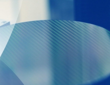
The EUV system works by projecting the light through a blueprint. Using a series of complex optics, made by German company Zeiss, the pattern is reduced and focused onto a thin slice of silicon coated with a light-sensitive chemical. The light interacts with the chemical effectively printing the pattern onto the silicon or wafer. When the unwanted silicon is etched away a three-dimensional structure is created. This is repeated dozens of times, layer upon layer, leaving a grid of hundreds of chips on one silicon wafer.
The light has to be focused in a vacuum to stop it being absorbed by air -- a difficult technological feat -- and the parameters are so small that the machine is working to within the size of an atom.
The tiniest speck of dust infiltrating the machine could ruin the design, leaving blank spaces on the chips.

