First Germanium Laser Bring Us Closer To Computers That Use Light Instead Of Electricity To Move Data
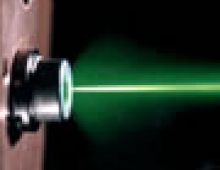
MIT researchers have demonstrated the first laser built from germanium that can produce wavelengths of light useful for optical communication.
It's also the first germanium laser to operate at room temperature. Unlike the materials typically used in lasers, germanium is easy to incorporate into existing processes for manufacturing silicon chips. So the result could prove an important step toward computers that move data - and maybe even perform calculations - using light instead of electricity. But more fundamentally, the researchers have shown that, contrary to prior belief, a class of materials called indirect-band-gap semiconductors can yield practical lasers.
As chips' computational capacity increases, they need higher-bandwidth connections to send data to memory. But conventional electrical connections will soon become impractical, because they'll require too much power to transport data at ever higher rates. Transmitting data with lasers - devices that concentrate light into a narrow, powerful beam - could be much more power-efficient, but it requires a cheap way to integrate optical and electronic components on silicon chips.
Chip assembly is a painstaking process in which layers of different materials are deposited on a wafer of silicon, and patterns are etched into them. Inserting a new material into this process is difficult: it has to be able to chemically bond to the layers above and below it, and depositing it must be possible at the temperatures and in the chemical environments suitable to the other materials.
The materials used in today's lasers, such as gallium arsenide, are "all tough fits," says Tremont Miao, a marketing director at Massachusetts-based Analog Devices Semiconductor. "They're all challenging integrations." As a consequence, the lasers have to be constructed separately and then grafted onto the chips, which is more expensive and time-consuming than building them directly on silicon would be. Moreover, gallium arsenide is much more expensive than silicon in the first place.
Integrating germanium into the manufacturing process, however, is something that almost all major chip manufacturers have already begun to do, since the addition of germanium increases the speed of silicon chips. "We and lots of other people know how to do that," Miao says.
Gallium arsenide, silicon, and germanium are all examples of semiconductors, the type of material used in virtually all modern electronics. Lasers made from semiconductors convert the energy of electrons'particles of charge into photons particles of light. Semiconductors come in two varieties: those with direct band gaps, like gallium arsenide, and those with indirect band gaps, like germanium and silicon. According to Jurgen Michel, principal research associate in the Electronic Materials Research Group and primary investigator on the germanium-laser project, "There was an opinion in the scientific area that indirect-band-gap semiconductors will never lase" ? that is, produce laser light. "That?s just what you teach in classes," says Lionel Kimerling, the Thomas Lord Professor of Materials Science and Engineering, who leads the group.
In a semiconductor crystal, an excited electron -one that'had energy added to it -will break free and enter the so-called conduction band, where it can move freely around the crystal. But in fact, an electron in the conduction band can be in one of two states. If it?s in the first state, and it falls out of the conduction band, it will release its extra energy as a photon. If it' in the second state, it will release its energy in other ways, such as heat.
In direct-band-gap materials, the first state -the photon-emitting state -is a lower-energy state than the second state; in indirect-band-gap materials, it' the other way around. An excited electron will naturally occupy the lowest-energy state it can find. So in direct-band-gap materials, excited electrons tend to go into the photon-emitting state, and in indirect-band-gap materials, they don'.
In a forthcoming paper in the journal Optics Letters, Kimerling, Michel and three other researchers in the group - ostdoc Jifeng Liu, the lead author on the paper, and grad students Xiaochen Sun and Rodolfo Camacho-Aguilera -describe how they coaxed excited germanium electrons into the higher-energy, photon-emitting state.
Their first strategy is a technique, common in chip manufacturing, called "doping," in which atoms of some other element are added to a semiconductor crystal. The group doped its germanium with phosphorous, which has five outer electrons. Germanium has only four outer electrons, "so each phosphorous gives us an extra electron," Kimerling says. The extra electron fills up the lower-energy state in the conduction band, causing excited electrons to, effectively, spill over into the higher-energy, photon-emitting state.
According to the group' theoretical work, phosphorous doping "works best at 1020 atoms per cubic centimeter" of germanium, Kimerling explains. So far, the group has developed a technique that can add 1019 phosphorous atoms to each cubic centimeter of germanium, "and we already begin to see lasing," Kimerling says.
The second strategy was to lower the energy difference between the two conduction-band states so that excited electrons would be more likely to spill over into the photon-emitting state. The researchers did that by adapting another technique common in the chip industry: they "strained" the germanium -or pried its atoms slightly farther apart than they would be naturally - growing it directly on top of a layer of silicon. Both the silicon and the germanium were deposited at high temperatures. But silicon doesn' contract as much as germanium when it cools. The atoms of the cooling germanium tried to maintain their alignment with the silicon atoms, so they ended up farther apart than they would ordinarily be. Changing the angle and length of the bonds between germanium atoms also changed the energies required to kick their electrons into the conduction band. "The ability to grow germanium on silicon is a discovery of this group," says Kimerling, "and the ability to control the strain of those germanium films on silicon is a discovery of this group."
"High-speed optical circuits like germanium in general," says Miao. "That' a good marriage and a good combination. So their laser research is very, very promising." Miao points out that the germanium lasers need to become more power-efficient before they'e a practical source of light for optical communications systems. "But on the other hand," he says, "the promise is exciting, and the fact that they got germanium to lase at all is very exciting."


