GLOBALFOUNDRIES Introduces New 12nm FinFET Technology
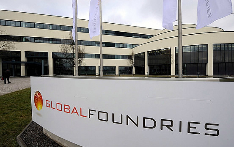
GlobalFoundries announced its new 12LP (leading performance) FinFET semiconductor manufacturing process designed to increase transistor density and improve frequency potential compared to GlobalFoundries' current-gen 14LPP tech.
The company expects the new process to be used by suppliers of various ICs (integrated circuits), including designers of CPUs and GPUs as well as developers of chips for automotive applications and telecommunication solutions. One of the first customers to adopt the 12LP fabrication process will be AMD.
The company says that the new 12LP technology provides as much as a 15 percent improvement in circuit density and more than a 10 percent improvement in performance over 16/14nm FinFET solutions on the market today. This positions 12LP to be fully competitive with other 12nm FinFET foundry offerings. The technology leverages GF's expertise at Fab 8 in Saratoga County, N.Y., where its 14nm FinFET platform has been in high-volume production since early 2016.
In addition to transistor-level enhancements, the 12LP platform will include new market-focused features specifically designed for automotive electronics and RF/analog applications:
- Emerging automotive applications in vehicle safety and automated driving require a combination of processing power and extreme reliability. The 12LP platform delivers both, with plans for Automotive Grade 2 qualification at Fab 8 by Q4 2017.
- A new RF offering extends the 12LP platform for RF/analog applications such as premium-tier transceivers in sub-6GHz wireless networks. GlobalFoundries claims that the 12LP offers the best scaling in both logic and memory for RF chip architectures with primarily digital and less RF/analog content.
GF's new 12nm FinFET technology complements its existing 12nm FD-SOI offering, 12FDX. 12FDX provides an alternative path for the next generation of connected intelligent systems, enabling the performance of 10nm FinFET with better power consumption, lower cost, and better RF integration than current-generation foundry FinFET offerings.
GlobalFoundries expects the new process to be used by suppliers of various ICs, including designers of CPUs and GPUs as well as developers of chips for automotive applications and telecommunication solutions. One of the first customers to adopt the 12LP fabrication process will be AMD.
The 12LP relies on deep ultraviolet (DUV) lithography with argon fluoride (ArF) excimer lasers operating on a 193 nm wavelength.
AMD will be one of the first to adopt the tech and accordimng to AMD CTO Mark Papermaster and Sunjay Jha, the chip developer will use the 12LP to make both CPUs and GPUs using the tech.
"We are pleased to extend our longstanding relationship with GlobalFoundries as a lead customer for their new 12LP technology," said Mark Papermaster, CTO and senior vice president of technology and engineering, AMD. "Our deep collaboration with GF has helped AMD bring a set of leadership high-performance products to market in 2017 using 14nm FinFET technology. We are excited to work with GF on its new 12LP process technology as a part of our focus on accelerating our product and technology momentum."
It is not clear whether AMD's forthcoming Vega 11 GPU is an 12LP product on the company's roadmap, or if AMD is planning on doing a more thorough refresh of Vega at 12LP later on.
GlobalFoundries expects to start risk production using the 12LP fabrication technology in Q1 2018.


