Imec Thin-film Image Sensor for the SWIR Could Make Smartphones and Autonomous Vehicles see the Impossible
Imec has developed a camera-integrated solution that uses Si-based CMOS sensors to detect short-wave infrared wavelengths that are normally out of reach for them because of physical and optical laws.
The development could open the way to extended functionalities in Augmented Reality, machine vision, autonomous vehicles etc.
CMOS technology has made visible imaging compact, low-power and affordable. Just about every smartphone now harbors a digital camera that’s capable of professional photography. But, the needs of the market are changing. Applications such as augmented reality and face recognition, autonomous driving and food scanning require a shift from imaging to sensing – from taking a picture to acquiring information.
The challenge is to bring these new imaging applications within reach of the consumer technology market, by lowering their cost without compromising their resolution. This is the goal of imec’s research activities, which break new ground in NIR/SWIR sensing and 3D imaging.
Research efforts involving material development, semiconductor processing skills, system-level design and more, have resulted to important breakthroughs in the capabilities of silicon-based CMOS imagers to detect short-wave infrared (SWIR) wavelengths above one micrometer. Such wavelengths (e.g. the 1450nm and 1550nm bands) are important for the development of applications such as computer vision in mobile devices. Yet, due to optical limitations, these wavelengths are normally invisible to Si-based devices. Conventional approaches that use III-V materials (e.g. InGaAs) can overcome this detection barrier, but are not available at an acceptable price point for consumer devices.
Thanks to thin-film photodetector (TFPD) technology, imec has developed an end-to-end solution that enables Si-based infrared CMOS sensors at the price level of conventional CMOS imagers. Initial results are being demonstrated up to the system-level via a camera-integrated solution.
Before getting into the technological details, let’s first have a short side-step to how your smartphone camera works. What’s obvious, is that it can detect and (thanks to the flashlight) emit visible light. What might be less obvious for some, is that it’s also active in the non-visible light spectrum. Not only as a detector, but also as a projector. For applications such as face recognition, your smartphone camera emits a grid dot pattern based on infrared light and captures the reflections coming from your face.
Typically, cameras to unlock your smartphone via face recognition are tuned to the near infrared (NIR) spectrum, more specifically the 940nm wavelength. This light is being absorbed by water, for example in the earth’s atmosphere. Which means you will get very little background noise or interference from radiation coming from the sunlight. Even though the human eye cannot consciously ‘see’ 940nm NIR, it is still sensitive to this frequency. This enforces limitations on the power that can be used to emit these signals and therefore on the useful application distance and efficiency in broad daylight. Face recognition works at maximum arm’s length; more advanced applications such as 3D scanning of objects and spaces don’t optimally function at larger distances.
A more ideal operational frequency for these scanning and sensing applications would be to move to the short-wave infrared (SWIR) spectrum. Here, the 1450nm band has similar advantages due to water absorption, yet less power restrictions due to several orders of magnitude lower sensitivity of the human eye. Also, in this SWIR spectrum lies the 1550nm band. Completely opposite to 940nm and 1450nm, this frequency is totally transparent to water, so in turn allows you to look through mist, clouds, smoke and water vapor. These frequencies allow to design devices that reach higher distances and have increased sensing capabilities, for example in (autonomous) vehicles flying through clouds or driving in bad weather conditions.
Unfortunately for image-sensor and application developers, silicon photodiodes cannot detect light with wavelengths above one micrometer. The basic silicon material is transparent for photons in this spectrum. Because of these physical limitations, conventional CMOS imagers are blind to SWIR radiation.
One well-known way to solve this is by using semiconductors that do allow for electrons to be excited by lower-energy photons. For example, sensors based on InGaAs or other III-V materials. While these technologies are already quite well developed, they lack the production throughput that is needed for consumer applications, and their system integration is not straightforward. This makes them too expensive for mass-manufacturing.
Imec has therefore come up with a solution that does allow for CMOS-based SWIR detection and this at the cost levels of silicon processing. Key enabler to achieve this are thin-film photodetectors (TFPD): multilayer stacks of a few hundred nanometers overall thickness with one of the layers being sensitive to IR. By post-processing these onto a Si-CMOS readout circuit, imec combines the best of both worlds: infrared detection via a CMOS-compatible process flow.
Regarding materials suitable for this thin film, imec is investigating multiple options, ranging from polymer- and small-molecule organic materials to inorganic colloidal quantum-dot layers. The latter, for the moment, is most promising because of the tunable and low-energy bandgap inherent to quantum dots. So far, imec has built most of its successful prototypes and demonstrators with PbS quantum-dot materials. The quantities of lead being used remain well within the legal restrictions of the EU ROHS guidelines and other regulations, making them suitable for production. Yet, completely lead-free alternatives are on imec’s roadmap and being investigated as well.

In view of future applications and product integration, imec follows a stepwise approach. In a first instance, monochrome infrared imagers based on a single TFPD stack are created and integrated as a separate die/functionality on the system level. This first implementation is the simplest, as it uses a plain, unpatterned layer of the thin-film photodetector stack. In this scenario, all pixels have the same absorption spectrum, unless you use specific filters. Potential application could be wavelength extension of the face scanner in smartphone cameras, allowing to move to the 1450nm spectrum without adding too much cost or complexity at the system level. Especially for Augmented Reality, this could become a valuable option to enable room-size scanning and applications.
In a second implementation, imec targets monolithically integrated TFPD stacks into the RGB pixel composition on the CMOS imager itself. In this design, an infrared subpixel can be added next to the conventional red, green and blue photodiodes. This means a separate sensor for IR detection would not be required, reducing both the system footprint and power consumption. Also, it would add an additional layer of information to visible cameras. Think for example about very accessible cameras with depth sensing capability.
The third implementation builds further on the monolithic pixelated design concept, combining multiple TFPD stacks with different active materials. Such configuration would enable pixel-level multispectral sensors in NIR and SWIR ranges, at a very compact form factor and a price point in the range of silicon image sensors. Application potential could be in autonomous vehicles needing long-range scanning capabilities (enabled by 1450nm-sensitive TFPD) as well as visibility in bad weather or low-light conditions (enabled by 1550nm-sensitive TFPD). Another application example could be in material sorting applications, where tuning pixels to characteristic wavelengths would add material-determination capabilities (e.g. discrimination of vegetation vs. buildings or real vs. fake plants).
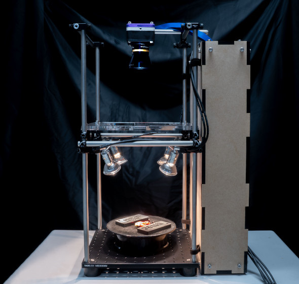
For the first concept – the monochromatic IR sensor – imec has built a complete end-to-end prototype integrated into a camera. Starting with a 200mm ROIC wafer processing in the foundry. Post-processing and TFPD integration (on die or wafer level) was executed in the imec fab, as well as chip packaging and buildup of the camera module. For the two monolithic designs, who are still in an earlier stage of research, the ambitions and roadmap are similar.


