Intel is Using EUV For Technology Development
Intel said that Extreme ultraviolet (EUV) lithography is “ready for introduction … and running in volume for technology development,” but does not confirm how or if EUV will be used for the company’s 10-nm products ramping now or its planned 7-nm node.
Speaking to EEtimes.com, Britt Turkot, a fellow and director of EUV at Intel, said that EUV lithography is that currently used at Intel's Portland, Oregon, fab, but engineers still face several challenges harnessing the complex and costly systems to make leading-edge chips in high volume.
Intel was among the semiconductor companies that helped pioneer the EUV technology but has been late in actually using it for the production of its chips.
On the other hand, rivals TSMC and Samsung have announced that they were ramping 7-nm nodes using EUV systems to print their finest features. But these companies still do not use 100% EUV equipment for their cutting edge chips.
TSMC’s N7+ is reportedly using EUV for only four metal layers. That means that it still requires use of double patterning with traditional immersion steppers for some metal layers. That's because of EUV’s high cost and maturity versus immersion. It's about throughput, how many EUV machines the company has, and cost trade-offs.
Samsung may have invested more in EUV machines, but declined to comment on its foundry pricing or how it uses EUV.
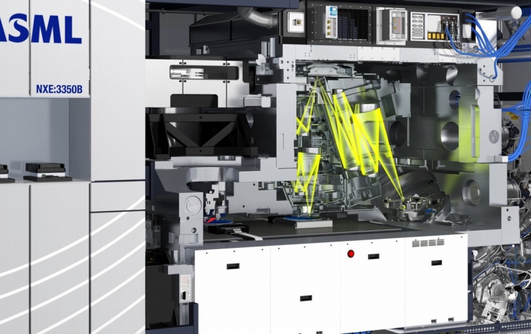
ASML's EUV systems cost about $150 million each, and several are needed for a commercial-production line.
Intel 's Turkot said that Intel has not yet decided on how many metal layers it will use with EUV, adding that choosing which layers to apply EUV is as much art as science. “Cost per layer is not a straightforward calculation — it’s not straight economics.”
For example, a single EUV exposure can sometimes reduce the mask count for a layer by a ratio of up to 5:1. However, double patterning with immersion steppers can help reduce edge-placement errors, she noted.
Regarding system reliability, Intel currently reports system uptime of about 75% to 80% for its EUV systems. “The number is not where it needs to be long term, but its good enough for introduction,” Turkot said. “We want it to be like immersion today, in the ’90s.”
On the other hand, Turkot says that the EUV equipment downtime is “more predictable.” “It was extremely unpredictable in the past, and [that made it] difficult to sustain a product line and run a volume line for development.”
Most of the reliability advances have come from “understanding the typical types of not-surprising tool downtime and building expertise to quickly diagnose issues and implement solutions necessary across the fleet.”
Much of the focus on EUV throughput has been on the power of the light source. It’s a critical and complex component that generates light by hitting a drop of molten tin with a laser. However, in practice, Turkot suggested that another EUV component — the light collector — is becoming a more important element in system throughput and uptime.
Intel has EUV systems running with power sources that range from 205 W to 285 W. At the level of the wafer, “they are all giving the same power because of the collector,” she said.“[But] wafer power changes day by day as the collector degrades.”
ASML is trying to tackle exposure source power and downtime issues by doing collector replacement. There’s a fixed overhead removing and replacing the collector and bringing the system back up and reducing the contamination rate.
Separately, ASML is now delivering protective films called pellicles. They keep wafers safe from fine particles that would otherwise contaminate them and lower yields.
Researchers are also concerned that random errors called stochastics that break or fail to complete a line drawn with an EUV system will limit their use at 5 nm and beyond. Improvements with EUV light and resist chemistry will be needed here in order to move to lower processes.


