ISSCC To Highlight Future Chip Advancements
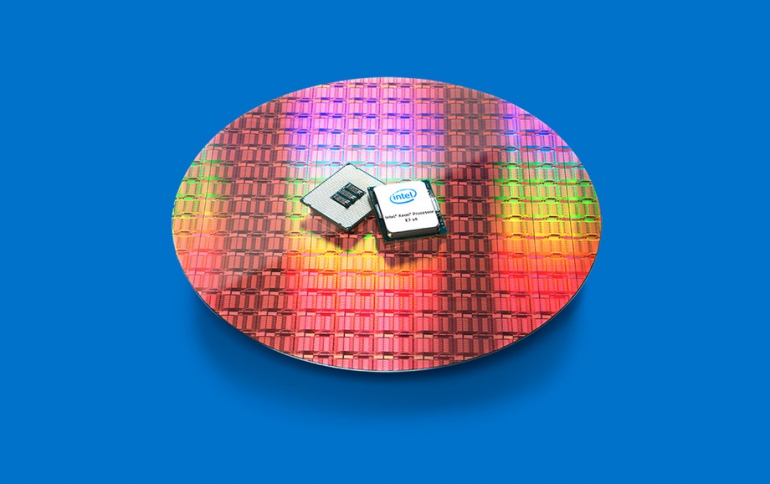
The 2016 IEEE international Solid-State Circuits Conference (ISSCC) will kick off Jan. 31 in San Francisco, CA, and technology giants will present papers describing the latest advancements - Samsung's and Intel's 10nm process technology, 3-D chip stacks, dense memories a 10-core SoC for mobiles, and more. According to the ISSCC program, Samsung will detail advances in DRAM and flash memory chips as well as a 128Mbit embedded SRAM made in a 10nm FinFET technology. ISSCC says the device has "the smallest [SRAM] bitcells to date," measuring 0.040µm for a high density (HD) and 0.049µm for a high current (HC) version. The designs sport "integrated assist circuitry that improves Vmin for the HD and HC bitcells by 130mV and 80mV, respectively."
TSMC, one of Samsung’s closest rivals in chip making, announced its 10nm process announced earlier this year. The Taiwan foundry is said to be gearing up the process to make the SoC inside Apple’s next-generation iPhone.
Intel as pushed back initial plans to make10nm chips, citing the increasing costs and complexity given delays in next-generation lithography needed to draw the finest lines. William M. Holt, general manager of Intel’s manufacturing group, will give a keynote entitled, "Moore’s Law: A Path Forward."
Besides describing Intel’s current 14nm process, the "talk will also discuss some leading technology options on the horizon beyond CMOS and their potential design benefits in advancing Moore’s Law well into the future. Novel 3D heterogeneous integration schemes and new memory technologies will be discussed for their potential in optimizing the memory hierarchy and addressing bandwidth challenges in processor performance and power," according to the ISSCC materials.
Besides squeezing more transoistors into to chip, an alternative way to to gain performance or lower power is to use 3-D stacks.
Samsung will describe a stack of up to eight DRAM chips that delivers bandwidth of 307 Gbits/s. Samsung put a phase-lock loop on the 20nm chip to ease testing of the device. To lower heat, it uses "an adaptive refresh scheme considering the [chip’s] temperature distribution," the paper description said.
South Korean SK Hynix will show a DRAM stack delivering 256 Gbit/s. The chip handles "command decoding and bias generation for the memory core…[at the] logic base-layer of the stack" instead of at the memory layer as in previous designs. In addition, it uses "small swing signaling on the heavily loaded [3-D interconnect] to reduce power for driving the interconnects."
Such dense memory chips will "enable high performance computing, accelerators and small form factor graphics cards," said ISSCC organizers.
A separate Samsung paper will describe a 256-Gbit flash chip storing three bits per cell and using an on-die stack of 48 cell layers.
Micron will describe a 768-Gbit flash chip with a 64KB page buffer in 179.2mm2 die area. It "achieves the highest density NAND flash memory by placing the peripheral circuits under the array."
Taiwanese Mediatek will present the "industry’s first tri-cluster, 10-core CPU, featuring three ARMv8a CPU clusters optimized for 1.4GHz, 2.0GHz, and 2.5GHz operation in a 20nm metal-gate process. Compared to dual-cluster CPUs, the addition of a third cluster provides 40% higher overall performance with 40% improved power efficiency," the program said.


