Panasonic Develops Next-generation Image Sensor
Panasonic today announced the development of a lightfast image sensor for the next generation.
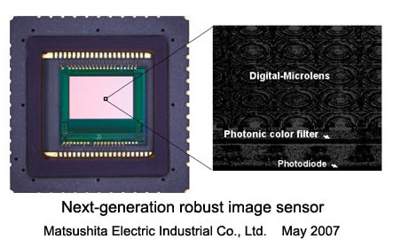
Panasonic claims that its technological breakthrough allows a robust MOS image sensor for use under harsh sunlight for more than 20 years. Unlike traditional image sensors with polymer onchip
microlenses and dyed color filters, the new MOS image
sensor has digital-microlenses and photonic color filters, both
made of inorganic materials that are inherently fade-resistant and
quite robust.
"We can make a significant contribution to our customers by creating new applications with this new sensor. We can also propose various market solutions like automobile and outdoor usages by making the most of its outstanding robustness," said Taku Gobara, Director of Corporate Application Specific Standard Products Division, Semiconductor Company, Matsushita Electric Industrial Co., Ltd.
Conventional MOS image sensors require polymer onchip microlenses and dyed RGB color filters, which are fragile and susceptible to sunlight exposure and a change in temperature. As a result, color images captured by a camera used under direct sunlight, including the ultra-violet (UV) portion, and higher temperature conditions will fade faster.
Panasinic's semiconductor process technology can realize the pattering of an array of digital-microlenses made of an inorganic material in subwavelength dimensions. A digital-microlens can be formed by patterning digitally the inorganic material in concentric rings, which works out as a conventional onchip microlens to gather more light onto the photo diode area. The light path of each digital-microlens can therefore readily be designed according to its relative position on the image area. As a result, a uniform sensitivity can be achieved across the image area in any camera module in use.
Furthermore, photonic color filters made of inorganic materials have been implemented for the first time by the photonic crystal technology, which allows the photonic color filters to select any colors form UV to infrared spectral regions. The photonic color filters can also provide a variety of camera modules with lightfastness that is essential for an increasing number of tough end uses such as security cameras and automotive cameras.
"We can make a significant contribution to our customers by creating new applications with this new sensor. We can also propose various market solutions like automobile and outdoor usages by making the most of its outstanding robustness," said Taku Gobara, Director of Corporate Application Specific Standard Products Division, Semiconductor Company, Matsushita Electric Industrial Co., Ltd.

Conventional MOS image sensors require polymer onchip microlenses and dyed RGB color filters, which are fragile and susceptible to sunlight exposure and a change in temperature. As a result, color images captured by a camera used under direct sunlight, including the ultra-violet (UV) portion, and higher temperature conditions will fade faster.
Panasinic's semiconductor process technology can realize the pattering of an array of digital-microlenses made of an inorganic material in subwavelength dimensions. A digital-microlens can be formed by patterning digitally the inorganic material in concentric rings, which works out as a conventional onchip microlens to gather more light onto the photo diode area. The light path of each digital-microlens can therefore readily be designed according to its relative position on the image area. As a result, a uniform sensitivity can be achieved across the image area in any camera module in use.
Furthermore, photonic color filters made of inorganic materials have been implemented for the first time by the photonic crystal technology, which allows the photonic color filters to select any colors form UV to infrared spectral regions. The photonic color filters can also provide a variety of camera modules with lightfastness that is essential for an increasing number of tough end uses such as security cameras and automotive cameras.


