Samsung Announces Production Start-up of Its Nonvolatile Memory - PRAM
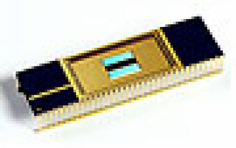
Samsung today announced at the sixth annual Samsung Mobile Solutions Forum held at the Westin Taipei Hotel that is has begun producing 512-Megabit (Mb) PRAM memory.
PRAM (phase change random access memory) is a new non-volatile memory technology that features high-performance and low power consumption. Samsung believes that will usher in the next generation of non-volatile memory technology for mobile devices.
High-density and high-performance are the key technology requirements for smartphones, however these attributes can increase power consumption significantly. Because PRAM?s greatly simplified data access logic requires less support from DRAM, its power usage is very efficient. By using PRAM, the battery life of a handset can be extended over 20 percent.
"We believe PRAM will make a highly significant contribution to the efficiency of mobile phone designs, particularly for multimedia handsets and smartphones," said Sei-Jin Kim, vice president, mobile memory planning and enabling group, Memory Division, Samsung Electronics. "We expect it to become one of our core memory products in the future."
The 512Mb PRAM can erase 64 Kilowords (KWs) in 80 milliseconds (ms), which is over 10 times faster than NOR flash memory. In data segments of 5 Megabytes (MBs), PRAM can erase and rewrite data approximately seven times faster than NOR flash.
More scalable than other memory architectures now under research, PRAM combines the speed of RAM for processing functions with the non-volatile characteristics of flash memory for storage.
Samsung's first PRAM is produced using 60-nanometer class technology, the same process technology used in NOR flash production today. Finer technology nodes will be applied in future generations of PRAM to expedite further commercial adoption.
Production of OneDRAM
 At the same event, Samsung also announced today that it has been ramping up production of its 1Gigabit (Gb) OneDRAM, a Samsung proprietary fusion memory, over the past two months.
"We are witnessing growing interest in the OneDRAM solution," said Sei-Jin Kim, vice president, mobile memory planning and enabling group, Memory Division, Samsung Electronics. "OneDRAM exemplifies our commitment to keep pace with innovative cell phone designs, in this instance by combining ultra-fast speeds and substantial power savings technology into an extremely efficient 1Gb package."
First introduced in 2008, the gain in operational efficiency using Samsung?s 60-nanometer (nm) class OneDRAM is especially beneficial in complex multimedia handset applications such as smartphones. The chip's 166MHz speed enables seamless operation with the processors, for full Internet browsing and teleconferencing.
Being showcased at the Mobile Solutions Forum, Samsung's 1Gb OneDRAM has a 1.3GBps data transfer speed, 20 percent faster than its previous 512Mb version. The OneDRAM chip is also seven times faster than a traditional dual-port RAM-based platform.
The smaller number of overall chips required in Samsung's OneDRAM-based platform allows use of a printed circuit board only two-thirds the size of those used in conventional handsets. For a more cost efficient solution, Samsung also provides its OneDRAM with a processor, NAND flash or OneNANDTM in a package-on-package (PoP) solution that measures 1.5mm in height and reduces the area coverage of the print circuit board by 40 percent. This PoP solution brings a seven-fold increase in performance with a 30 percent decrease in power usage.
The OneDRAM's internal interface, which complies with the JEDEC low-power, double-data-rate (LPDDR) memory standard, channels data between the processors through a shared data area in the OneDRAM chip, eliminating the need for DRAM and double-port RAM chips when transferring data.
High-density and high-performance are the key technology requirements for smartphones, however these attributes can increase power consumption significantly. Because PRAM?s greatly simplified data access logic requires less support from DRAM, its power usage is very efficient. By using PRAM, the battery life of a handset can be extended over 20 percent.
"We believe PRAM will make a highly significant contribution to the efficiency of mobile phone designs, particularly for multimedia handsets and smartphones," said Sei-Jin Kim, vice president, mobile memory planning and enabling group, Memory Division, Samsung Electronics. "We expect it to become one of our core memory products in the future."
The 512Mb PRAM can erase 64 Kilowords (KWs) in 80 milliseconds (ms), which is over 10 times faster than NOR flash memory. In data segments of 5 Megabytes (MBs), PRAM can erase and rewrite data approximately seven times faster than NOR flash.
More scalable than other memory architectures now under research, PRAM combines the speed of RAM for processing functions with the non-volatile characteristics of flash memory for storage.
Samsung's first PRAM is produced using 60-nanometer class technology, the same process technology used in NOR flash production today. Finer technology nodes will be applied in future generations of PRAM to expedite further commercial adoption.
Production of OneDRAM
 At the same event, Samsung also announced today that it has been ramping up production of its 1Gigabit (Gb) OneDRAM, a Samsung proprietary fusion memory, over the past two months.
"We are witnessing growing interest in the OneDRAM solution," said Sei-Jin Kim, vice president, mobile memory planning and enabling group, Memory Division, Samsung Electronics. "OneDRAM exemplifies our commitment to keep pace with innovative cell phone designs, in this instance by combining ultra-fast speeds and substantial power savings technology into an extremely efficient 1Gb package."
First introduced in 2008, the gain in operational efficiency using Samsung?s 60-nanometer (nm) class OneDRAM is especially beneficial in complex multimedia handset applications such as smartphones. The chip's 166MHz speed enables seamless operation with the processors, for full Internet browsing and teleconferencing.
Being showcased at the Mobile Solutions Forum, Samsung's 1Gb OneDRAM has a 1.3GBps data transfer speed, 20 percent faster than its previous 512Mb version. The OneDRAM chip is also seven times faster than a traditional dual-port RAM-based platform.
The smaller number of overall chips required in Samsung's OneDRAM-based platform allows use of a printed circuit board only two-thirds the size of those used in conventional handsets. For a more cost efficient solution, Samsung also provides its OneDRAM with a processor, NAND flash or OneNANDTM in a package-on-package (PoP) solution that measures 1.5mm in height and reduces the area coverage of the print circuit board by 40 percent. This PoP solution brings a seven-fold increase in performance with a 30 percent decrease in power usage.
The OneDRAM's internal interface, which complies with the JEDEC low-power, double-data-rate (LPDDR) memory standard, channels data between the processors through a shared data area in the OneDRAM chip, eliminating the need for DRAM and double-port RAM chips when transferring data.


