Samsung Has Started 3D V-NAND Production In Chinese Facility
Samsung Electronics has started operating its 3D V-NAND memory fabrication line in Xi'an China in full-scale.
Construction of the new manufacturing facility took 20 months since Samsung broke ground here in September, 2012. The total area of the facility is approximately 230,000 square meters, situated on 1.14 million square meters of land.
Samsung Vice Chairman and CEO Dr. Oh-Hyun Kwon hosted a plant inauguration event, which welcomed a large number of attendees including Chinese government dignitaries.
By commencing operations of its Xi'an fabrication line, Samsung has secured a solid memory production base in China, a market where approximately 50 percent of global NAND flash is generated from production bases operated by many IT companies here.
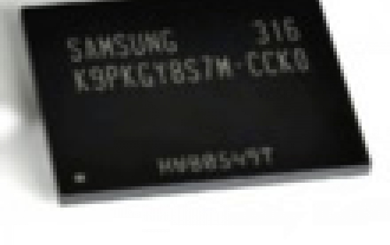
Samsung's three-dimensional (3D) Vertical NAND (V-NAND) flash memory will be used for a wide range of consumer electronics and enterprise applications, including embedded NAND storage and solid state drives (SSDs). It offers a 128 gigabit (Gb) density in a single chip, utilizing the company's proprietary vertical cell structure based on 3D Charge Trap Flash (CTF) technology and vertical interconnect process technology to link the 3D cell array. By applying both of these technologies, Samsung's 3D V-NAND is able to provide over twice the scaling of 20nm-class planar NAND flash.
Samsung plans to complete construction of its entire Xi'an complex, which includes an assembly facility and test line, by the end of this year.


