Samsung Introduces Tbit V-NAND Memory Solutions
Samsung unveiled plans for a terabit 3D-NAND chip that it will ship next year as well as dense solid-state drives using its current chips. It also said that it is sampling the Z-NAND products at latency levels that match or beat Intel's 3DXP memories.
At the inaugural Samsung Tech Day and this year's Flash Memory Summit, Samsung announced a 1Tb V-NAND chip. Initially mentioned in 2013, during unveiling of the first 3D NAND, Samsung has been working to enable its core memory technologies to realize one terabit of capacity on a single chip using a V-NAND structure.
The arrival of a 1Tb V-NAND chip next year will enable 2TB of memory in a single V-NAND package by stacking 16 1Tb dies and will represent one of the most important memory advances of the past decade.

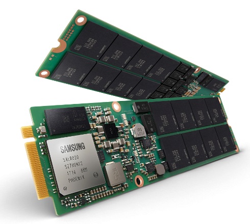
Samsung is also sampling the first 16-terabyte (TB) NGSFF SSD, which will improve the memory storage capacity and IOPS (input/output operations per second) of today's 1U rack servers. Measuring 30.5mm x 110mm x 4.38mm, the Samsung NGSFF SSD provides hyper-scale data center servers with substantially improved space utilization and scaling options.
Utilizing the new NGSFF drive instead of M.2 drives in a 1U server can increase the storage capacity of the system by four times. To highlight the advantages, Samsung demonstrated a reference server system that delivers 576TB in a 1U rack, using 36 16TB NGSFF SSDs. The 1U reference system can process about 10 million random read IOPS, which triples the IOPS performance of a 1U server equipped with 2.5-inch SSDs. A petabyte capacity can be achieved using only two of the 576TB systems.
Samsung plans to begin mass producing its first NGSFF SSDs in the fourth quarter of this year, while working to standardize the form factor with industry partners.
Following last year's introduction of its Z-SSD technology, Samsung introduced its first Z-SSD product, the SZ985. Featuring ultra-low latency and high performance, the Z-SSD will be used in data centers and enterprise systems dealing with extremely large, data-intensive tasks such as real-time "big data" analytics and high-performance server caching.
The Samsung SZ985 requires only 15 microseconds of read latency time which is approximately a seventh of the read latency of an NVMe SSD. At the application level, the use of Samsung's Z-SSDs can reduce system response time by up to 12 times, compared to using NVMe SSDs. The chips use sense amps optimized solely for latency, run at data rates up to 800 Mbits/s, and target data centers running analytics and caching programs.
The Z-NAND products challenge Intel's Optane SSDs based on its 3DXP chips and launched in March. Given the latencies of the PCI Express bus that SSDs use, the most disruptive opportunities for such chips will be in cards expected next year riding faster memory busses.
Samsung also introduced a new technology called Key Value SSD. The name refers to a method of processing complex data sets.
Today, SSDs convert object data of widely ranging sizes into data fragments of a specific size called "blocks." The use of these blocks requires implementation processes consisting of LBA (logical block addressing) and PBA (physical block addressing) steps. However, Samsung's new Key Value SSD technology allows SSDs to process data without converting it into blocks. Samsung's Key Value instead assigns a 'key' or specific location to each "value," or piece of object data - regardless of its size. The key enables direct addressing of a data location, which in turn enables the storage to be scaled. Samsung's Key Value technology enables SSDs to scale-up (vertically) and scale-out (horizontally) in performance and capacity. As a result, when data is read or written, a Key Value SSD can reduce redundant steps, which leads to faster data inputs and outputs, as well as increasing TCO and significantly extending the life of an SSD.


