Samsung Starts Commercial Shipment of eMRAM Product Based on 28nm FD-SOI Process
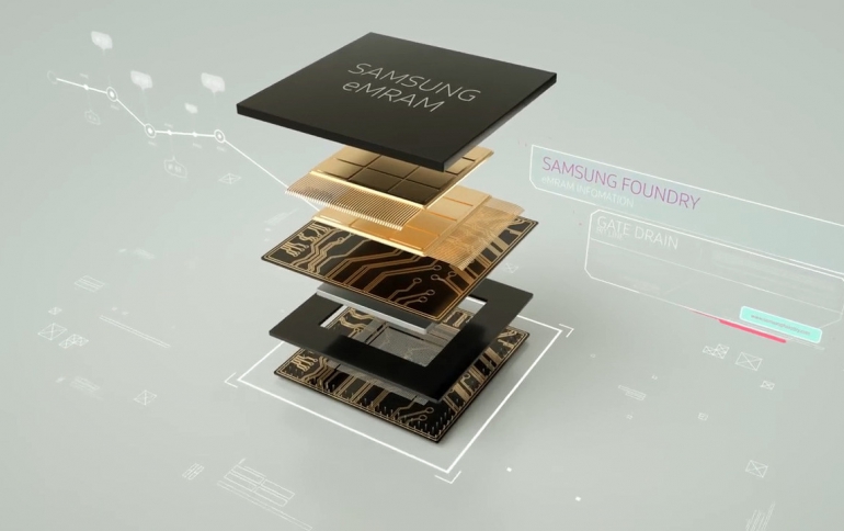
Samsung Electronics has commenced mass production of its first commercial embedded magnetic random access memory (eMRAM) product based on the company’s 28-nanometer(nm) fully-depleted silicon-on-insulator (FD-SOI) process technology, called 28FDS.
As eFlash has faced scalability challenges due to a charge storage-based operation, eMRAM has been the most promising successor since its resistance-based operation allows strong scalability while also possessing outstanding technical characteristics of memory semiconductors such as nonvolatility, random access, and strong endurance.
Samsung says that its 28FDS-based eMRAM solution offers power and speed advantages with lower cost. Since eMRAM does not require an erase cycle before writing data, its writing speed is approximately a thousand times faster than eFlash. Also, eMRAM uses lower voltages than eFlash, and does not consume electric power when in power-off mode, resulting in power efficiency.
Furthermore, since an eMRAM module can be inserted in the back-end of the process by adding the least number of layers, it has less dependence on the front-end of the process for easy integration with existing logic technologies, such as bulk, fin, and FD-SOI transistor.
By combining with 28FD-SOI for better transistor control and minimizing leakage current through body-bias control, Samsung’s eMRAM solution is expected to provide differentiated benefits for a variety of applications including micro controller unit (MCU), internet of things (IoT), and artificial intelligence (AI).
Samsung plans to expand its options for high-density eNVM solutions, including a tape-out of 1Gb eMRAM test chip within this year.


