Scientists Set New Speed Record for Big Data
IBM has achieved a new technological advancement that will help improve Internet speeds to 200 - 400 Gigabits per second (Gb/s) at extremely low power. The speed boost is based on a device that can be used to improve transferring Big Data between clouds and data centers four times faster than current technology. At this speed 160 Gigabytes, the equivalent of a two-hour, 4K ultra-high definition movie or 40,000 songs, could be downloaded in only a few seconds. The device was presented at the International Solid-State Circuits Conference (ISSCC) in San Francisco.
While this latest technology is a lab prototype, a previous version of the design has been licensed to Semtech Corp., a supplier of analog and mixed-signal semiconductors. The company is using the technology to develop advanced communications platforms expected to be announced later this year.
Scientists at IBM Research and Ecole Polytechnique Fédérale de Lausanne (EPFL) have been developing ultra-fast and energy efficient analog-to-digital converter (ADC) technology to enable complex digital equalization across long-distance fiber channels.
An ADC converts analog signals to digital, approximating the right combination of zeros and ones to digitally represent the data so it can be stored on computers and analyzed for patterns and predictive outcomes.
For example, scientists will use hundreds of thousands of ADCs to convert the analog radio signals that originate from the Big Bang 13 billion years ago to digital. It’s part of a collaboration called Dome between ASTRON, the Netherlands Institute for Radio Astronomy, DOME-South Africa and IBM to develop a fundamental IT roadmap for the Square Kilometer Array (SKA), an international project to build the world’s largest and most sensitive radio telescope.
The radio data that the SKA collects from deep space is expected to produce 10 times the global internet traffic and the prototype ADC would be an ideal candidate to transport the signals fast and at very low power — a critical requirement considering the thousands of antennas which will be spread over 3,000 kilometers (1,900 miles).
Semtech signed a non-exclusive technology licensing agreement, including access to patented designs and technological know-how, with IBM to develop the technology for its own family of products ranging from optical and wireline communications to advanced radar systems.
"Through leveraging the IBM 32nm SOI process with its unique feature set, we are developing products that are well-suited for meeting the challenge presented by the next step in high performance communications systems such as 400 Gb/s Optical systems and Advanced Radar systems. We are also seeing an expanding range of applications in the existing radio frequency communications marketplace where high-speed digital logic is replacing functions that have been traditionally performed by less flexible analog circuitry," said Craig Hornbuckle, Chief Systems Architect, Semtech.
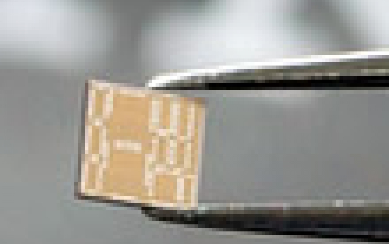
The 64 GS/s (giga-samples per second) chips for Semtech will be manufactured at IBM’s 300mm fab in East Fishkill, New York in a 32 nanometer silicon-on-insulator CMOS process and has an area of 5 mm2. This core includes a wide tuning millimeter wave synthesizer enabling the core to tune from 42 to 68 GS/s per channel with a nominal jitter value of 45 femtoseconds root mean square. The full dual-channel 2x64 GS/s ADC core generates 128 billion analog-to-digital conversions per second, with a total power consumption of 2.1 Watts.


