Toshiba Announces 96-Layer 3D Flash Memory and 64-Layer QLC 3D Flash Memory
Toshiba has developed a prototype sample of 96-layer BiCS FLASH three-dimensional (3D) flash memory with a stacked structure with 3-bit-per-cell (TLC) technology. In addition, the company unveiled the first BiCS FLASH 3D flash memory with a stacked cell structure based on the 4-bit-per-cell (QLC) technology.
96-layer BiCS FLASH with TLC
Toshiba, along with its partner Western Digital, will start providing samples of the new 96-layer product, which is a 256 gigabit (32 gigabytes) device, in the second half of 2017. Mass production is targeted for 2018.
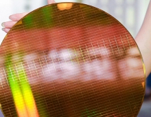
BiCS FLASH three-dimensional (3D) flash memory is a structure stacking Flash memory cells vertically on a silicon substrate to realize density improvements over planar NAND Flash memory, where cells are formed on the silicon substrate.
Going forward, Toshiba will apply its new 96-layer process technology to larger capacity products, such as 512 gigabit (64 gigabytes) and 4-bit-per-cell (quadruple-level cell, QLC) technology, in the near future.
The 96-layer stacking process combines with advanced circuit and manufacturing process technology to achieve a capacity increase of approximately 40% per unit chip size over the 64-layer stacking process. It reduces the cost per bit, and increases the manufacturability of memory capacity per silicon wafer.
This 96-layer BiCS FLASH will be manufactured at Yokkaichi Operations in Fab 5, the new Fab 2, and Fab 6, which will open in summer 2018.
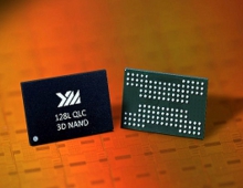
First QLC 3D Flash Memory
Toshiba has also developed the first BiCS FLASH three-dimensional (3D) flash memory with a stacked cell structure. The newest BiCS FLASH device features 4-bit-per-cell, quadruple-level cell (QLC) technology, advancing capacity beyond that of triple-level cell (TLC) devices and pushing the boundaries of flash memory technology.
Multi-bit cell flash memories store data by managing the number of electrons in each individual memory cell. Achieving QLC technology posed a series of technical challenges, as increasing the number of bit-per-cell by one within same electron count requires twice the accuracy of TLC technology. Toshiba says it has drawn on its advanced circuit design capabilities and 64-layer 3D flash memory process technology to create the QLC 3D flash memory.
The prototype features the world's largest die capacity (768 gigabits/96 gigabytes) with 64-layer 3D flash memory process. Shipment of prototypes to SSD and SSD controller vendors for evaluation and development purposes started in early June.
The QLC 3D flash memory also enables a 1.5-terabyte (TB) device with a 16-die stacked architecture in a single package - the industry's largest capacity. Toshiba will showcase samples of this device will be showcased at the 2017 Flash Memory Summit in Santa Clara, California, United States, from August 7-10.
"The introduction of QLC technology sets the stage for solving many of the challenges facing datacenters today," noted Greg Wong, founder and principal analyst at Forward Insights. "For datacenters, QLC SSDs can be an excellent design choice for reducing power consumption and lowering footprint. Additionally, as the push for higher capacity HDDs leads to an increase in areal density and drives up the weight per successive generation, it has become common to see a 42U rack only half-filled due to exceeding maximum weight or power supply. Flash memory-based storage solutions weigh less and realize improved power efficiencies, enabling datacenters to achieve maximum rack capacity."
New investments in manufacturing facilities for Fab 6 at Yokkaichi Operations
Toshiba's board of directors, meeting today, has agreed upon a FY2017 investment program for its wholly owned subsidiary, Toshiba Memory Corporation (TMC), that will channel approximately 180 billion yen into Fab 6 at Yokkaichi Operations, TMC's Flash memory facility. The investment will cover installation of manufacturing facilities in Phase-1 of the fab, and the construction of Phase-2.
Toshiba sid that production at Fab 6 would be entirely devoted to BiCS FLASH. Phase-1 of the fab is scheduled for completion in summer 2018, and the current round of investment will ensure this target date is met.
The investment in Fab 6 will enable TMC to install manufacturing equipment for 96-layer 3D Flash memories, including deposition and etching equipment. In parallel with this, construction of Phase-2 of Fab 6 is scheduled to start in September this year, with a completion target of the end of 2018.
TMC has recently asked SanDisk, its partner in joint ventures for investment in manufacturing equipment at TMC's Yokkaichi Operations, to clarify whether it intends to jointly invest in the Fab 6 facility. If SanDisk does not agree to such joint investment, TMC said it would invest alone in manufacturing equipment for separate TMC capacity.