Toshiba Develops New NAND Flash Technology
Toshiba today announced a new three dimensional memory cell array structure that enhances cell density and data capacity without relying on advances in process technology, and with minimal increase in the chip die size.
Toshiba announced its new development at the VLSI symposium on June 12.
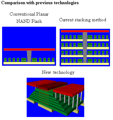
In the new structure, pillars of stacked memory elements pass vertically through multi-stacked layers of electrode material and utilize shared peripheral circuits. The new design is a potential candidate technology for meeting future demand for higher density NAND flash memory.
Typically, advances in memory density reflect advances in process technology. Toshiba's new approach is based on innovations in the stacking process. Existing memory stacking technologies simply stack two-dimensional memory array on top of another, repeating the same set of processes. While this achieves increased memory cell density, it makes the manufacturing process longer and more complex. The new array does increase memory cell density, is easier to fabricate, and does not produce much increase in chip area, as peripheral circuits are shared by several silicon pillars.
Toshiba said that it would further develop this technology to the level where it wouold be secure and reliabile.
In the new structure, pillars of stacked memory elements pass vertically through multi-stacked layers of electrode material and utilize shared peripheral circuits. The new design is a potential candidate technology for meeting future demand for higher density NAND flash memory.
Typically, advances in memory density reflect advances in process technology. Toshiba's new approach is based on innovations in the stacking process. Existing memory stacking technologies simply stack two-dimensional memory array on top of another, repeating the same set of processes. While this achieves increased memory cell density, it makes the manufacturing process longer and more complex. The new array does increase memory cell density, is easier to fabricate, and does not produce much increase in chip area, as peripheral circuits are shared by several silicon pillars.

Toshiba said that it would further develop this technology to the level where it wouold be secure and reliabile.


