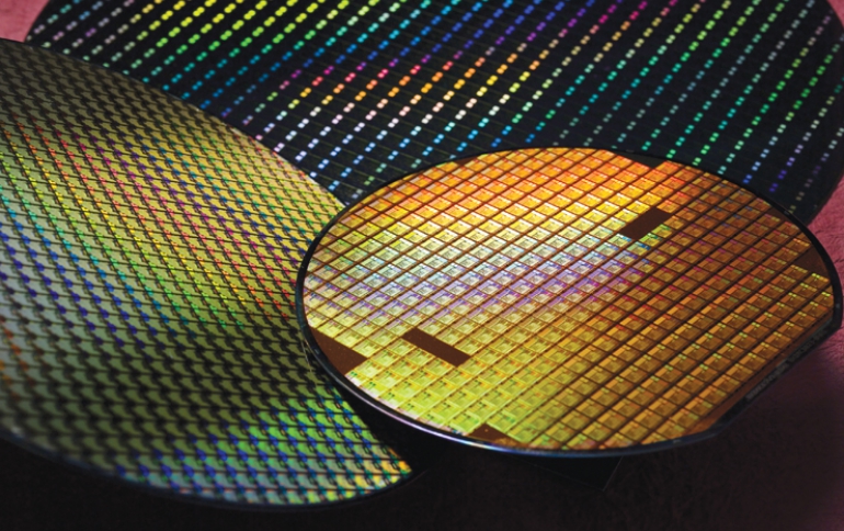
Samsung Says Semiconductor Technology Can Easily Scale Down to 5nm
Despite concerns for the demise of scaling, Samsung says that high performance in electronics systems for the coming decades is expected, thanks to innovations in materials, structures and processes. Kinam Kim, president of Samsung Electronics, discussed the latest trends of semiconductor scaling techniques and the development status at the company during a keynote speech at 2015 IEEE International Solid-State Circuits Conference (ISSCC).
Kim spoke on the potentials of semiconductor technologies, saying, "They can be scaled down to 5nm without any fundamental technical difficulty, and further scaling is possible."
He announced that Samsung has already prototyped a device featuring FinFET with a gate length of just 3.8nm. In terms of the resolution of lithography technology for semiconductor volume production, it is possible to realize a resolution of 3.25mm by combining EUV (extreme ultraviolet) and quadruple patterning, Kim said. Though the resolution of resist technology is currently 8nm, it will be further scaled down because the company is currently developing a resist material for EUV technology, he said.
Samsung semiconductor started volume production of FinFET using 14nm process technology in January 2015. Though they can be scaled down to about 7nm with FinFET, GAA (gate all around) and tunnel FET will be the mainstream after that, Kim said.
Regarding DRAM, Samsung is currently using 20nm process technology, but it is possible to realize 1Xnm process technology, Kim said.
"If the current planar NAND technology is further scaled down, the capacity coupling with the surroundings of elements will rapidly increase," Kim said, indicating that process scale-down is getting stuck at 1Xnm.
Vertical NAND (V-NAND) has small capacity coupling with the surroundings and is a promising candidate for high-density and multi-valued 3D stacking. The maximum number of the layers of 3D V-NAND was 24 in 2013 abd was further increased to 32 in 2014.
"The number of layers will be larger than 40 in 2015 and larger than 100 in the future, making it possible to develop a 1-Tbit 3D V-NAND chip," Kim said.