Fujitsu Develops Optical Transceiver for 400 Gbps Inter-Processor Data Transmissions
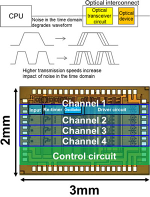
Fujitsu Laboratories today announced the development of the first optical transceiver circuit in which multiple circuit lanes can be laid out in parallel, paving the way for higher-capacity data transmissions between CPUs in future servers and supercomputers. Re-timer circuits handle the waveform and noise reduction needed for high-density transmitter circuit and high-speed transmission signals. Because individual re-timer circuits are susceptible to coupling from adjacent ones, it has been difficult to lay them out in close proximity to each other. While the transmitter/receiver circuit width can be adjusted down to 0.25 mm, the typical pitch of laid out optical fibers, the re-timer circuit required a pitch of at least 0.5 mm.
 By developing a mathematical model and analytic techniques for the impact of mutual coupling between re-timer circuits, Fujitsu Laboratories succeeded in laying out, for the first time in the world, re-timer circuits with spacing of just 0.25 mm, the same distance between optical fibers. This result enables optical transceiver circuits to integrate with high density.
In tests of this technology, transmission bandwidth of 100 Gbps (25Gbps x 4) was confirmed by running four lanes of an optical transceiver circuit with an integrated re-timer circuit and an optical device. Using this optical transceiver circuit with an integrated re-timer circuit and optical device in a 16-lane configuration will enable 400 Gbps next-generation interconnects, which can be utilized for data transmissions between future servers and the high-volume data transmissions of next-generation supercomputers.
Fujitsu Laboratories is aiming to bring higher-capacity optical interconnects for servers into practical implementation in fiscal 2016, and is working to develop compact optical interconnect technology.


