GLOBALFOUNDRIES Announces Strategic Customer Engagement with STMicroelectronics
GLOBALFOUNDRIES today announced a strategic customer relationship with STMicroelectronics.
ST will partner with GLOBALFOUNDRIES to produce products based on 40nm Low Power (LP) bulk silicon technology. The 40nm LP process is ideal for the next generation of wireless applications, handheld devices, and consumer electronics, which require excellent performance and long battery life. First tape out and production of ST products by GLOBALFOUNDRIES is planned to start in 2010.
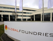
GLOBALFOUNDRIES production is currently centered at a 300mm manufacturing campus in Dresden, Germany otherwise known as Fab 1. Consistently ranked as one of the top fabs in the industry, Fab 1 has a proven track record of ramping leading-edge technologies at high-volume and mature yields, most recently evidenced on a seamless ramp of 45nm process technology. In July 2009, GLOBALFOUNDRIES also broke ground on Fab 2, a $4.2B wafer manufacturing facility in Malta, N.Y. Once complete, Fab 2 is expected to be the most advanced semiconductor foundry in the world.
GLOBALFOUNDRIES production is currently centered at a 300mm manufacturing campus in Dresden, Germany otherwise known as Fab 1. Consistently ranked as one of the top fabs in the industry, Fab 1 has a proven track record of ramping leading-edge technologies at high-volume and mature yields, most recently evidenced on a seamless ramp of 45nm process technology. In July 2009, GLOBALFOUNDRIES also broke ground on Fab 2, a $4.2B wafer manufacturing facility in Malta, N.Y. Once complete, Fab 2 is expected to be the most advanced semiconductor foundry in the world.


