IBM Develops 7nm Processor
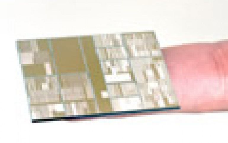
IBM said on Thursday that it had made working versions of ultradense computer chips made usunbg an 7nm manufacturing process - roughly four times the capacity of today’s most powerful chips. The announcement is part of an effort to manufacture the most advanced computer chips in New York’s Hudson Valley, where IBM is investing $3 billion in a private-public partnership with New York State, GlobalFoundries, Samsung and equipment vendors.
The race to cmake the Moore Law continue past the current 14- nanometer generation of chips is in progress. The industry is making the commercial transition from what the industry generally describes as 14-nanometer manufacturing to 10-nanometer manufacturing.
Although the 7nm chips are not yet ready for commercial manufacturing, the working samples made the research advance by using silicon-germanium instead of pure silicon in key regions of the molecular-size switches.
The new material makes possible faster transistor switching and lower power requirements. The tiny size of these transistors suggests that further advances will require new materials and new manufacturing techniques.
The IBM Research-led alliance achieved close to 50 percent area scaling improvements over today’s most advanced technology, introduced SiGe channel material for transistor performance enhancement at 7nm node geometries, process innovations to stack them below 30nm pitch and full integration of EUV lithography at multiple levels. These techniques and scaling could result in at least a 50 percent power/performance improvement for next generation mainframe and POWER systems that will power the Big Data, cloud and mobile era.
IBM now licenses the technology it is developing to a number of manufacturers and GlobalFoundries, to make chips for companies including Broadcom, Qualcomm and Advanced Micro Devices.
This year, Taiwan Semiconductor Manufacturing Company said that it planned to begin pilot product of seven-nanometer chips in 2017.
It is uncertain whether the longer exposure times required by the new generation of EUV photolithographic stepper machines would make high-speed manufacturing operations impossible. Even the slightest vibration can undermine the precision of the optics necessary to etch lines of molecular thicknesses, and the semiconductor industry has been forced to build specialized stabilized buildings to try to isolate equipment from vibration.
An IBM official said that the consortium now sees a way to use EUV
light in commercial manufacturing operations.


