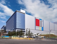
IC Knowledge Outlines EUV, 7nm and 5nm Progress
The latest Extreme ultraviolet lithography (EUV) equipment is set to enable 10nm and 7nm process nodes over the next years, although the transition to the 5nm node with EUV needs futher work.
Speaking to the SEMI Industry Strategy Symposium (ISS) in San Franscisco, Scotten Jones, president of IC Knowledge, talked about the advantages of EUV but underlined that existing chip making equipment and gear will be still needed in tandem with EUV for future process nodes.
He said that EUV provides a great reduction in cycle time and edge placement errors, but not much cost reduction, at least initially. To enable 5nm chips, pellicles, mask testers and resists are among the top concerns outside the EUV system, he added.
"The main pieces for EUV at 7nm are in place, and we will see some volume of wafers this year, but photoresist defects are still an order of magnitude too high for 5nm," said Jones.
For those not familiar with EUV, reducing defects on EUV masks is currently one of the most critical issues to be addressed for commercialization of EUV lithography, since even defects of atomic scale height can still be printable.
In addition, production EUV tools need a pellicle to protect the mask from contamination. Ideally, the pellicle should be guaranteed to withstand 250 W power necessary for high volume manufacturing. But this is not the case so far.
Pellicles are normally expected to protect the mask from particles during transport, entry into or exit from the exposure chamber, as well as the exposure itself. However, for EUV, the feasibility of pellicle use is severely challenged, due to the required thinness of the shielding films to prevent excessive EUV absorption. Particle contamination would be prohibitive if pellicles were not stable above 200 W, i.e., the targeted power for manufacturing.
Heating of the EUV mask pellicle is a significant concern, due to the resulting deformation and transmission decrease.
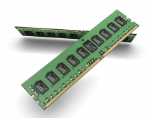
EUV maker ASML has announced it shipped 10 EUV systems last year and will ship 20-22 more this year. The systems will have or at least support a 250W laser light source needed to produce 125 wafers/hour. They will first be used on logic chips such as microprocessors and later applied to DRAMs but are not needed by today's 3D NAND flash chips, Scotten said.
ASML has plans in place to increase uptime of the systems from about 75 percent today to 90 percent. In addition, the company will release in time a pellicle needed to protect some EUV wafers from contamination.
ASML aims to boost the 145 wafers/hour throughput it can get with its 250W light source to 155 w/h in 2020. It has demonstrated a 375W light source working in the lab, said Peter Jenkins, ASML's vice president for corporate strategy and marketing.
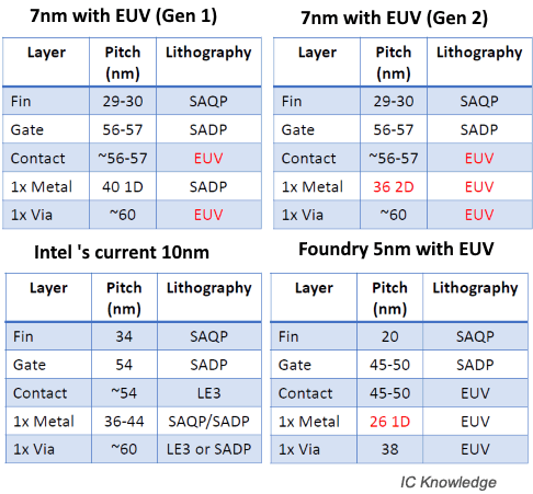
Jones said that TSMC qualified last fall a 7nm process that is ramping now using existing optical steppers. Globalfoundries will ramp a similar process later this year, he said.
Both companies plan to ramp next year a second-generation 7nm process using EUV to make contacts and vias, reducing 15 optical layers to five EUV layers. The process does not need a pellicle.
GF announced last June its 2019 plan for 7nm with EUV. TSMC is also said to do this.
Chip makers will probably have to use e-beam systems to insect masks for defects. The technology employs a high resolution electron beam to induce a local chemical reaction on the EUV mask surface. More accurate actinic systems are still in the works. These look for defects using the same 13.5 mm wavelength as the EUV systems.
In addition, GF, Samsung and TSMC plan 7nm variants that use EUV with a pellicle to make a first metal layer.
This is the approach Samsung will use for its first 7nm node, called 7LPP, due early next year. TSMC will call its version 7FF+ and ramp it in mid-2019 and GF will follow with its 7LP+ late next year, Jones added.
Jones also said that Intel's 10nm process offers similar density to what its rivals plan with their best 7nm variants. Intel's approach is using optical steppers, but Jones expects that Intel will adopt EUV for a 10nm+ upgrade in 2019.
Samsung and TSMC are already talking about 5nm processes that could be available before the end of 2019. They could be the first to use EUV for 1D metal layers.