New 3D Memory Package Improves Performance Using Less Space
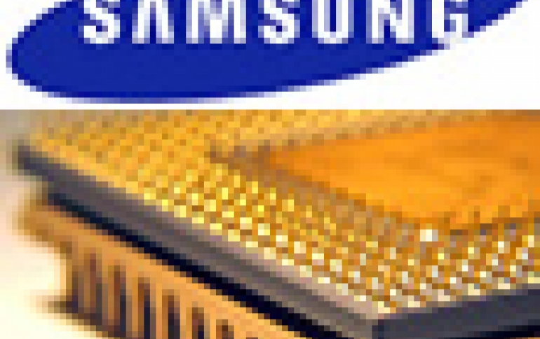
Samsung announced today that it has developed a new stacking technology for semiconductior chips, which offer a small footprint and improved overall performance.
The Korean company will apply the new wafer-level processed stack package (WSP) technology to the production of NAND-based memory cards for mobile applications and other consumer electronics in early 2007.
WSP can be applied to all types of hybrid packages, including memory and processors, to deliver higher speed and higher density with minimum use of chip space. The technology allows mobile device and consumer electronics manufacturers will gain better electrical performance, well suited for slimmer, high-performance handset designs that provide longer battery time.
The WSP generates a much smaller multi-chip package (MCP), which is the current mainstream solution for designing miniaturized, high-capacity memory devices. The chips in today's multi-chip packages (MCPs) are connected by wire bonding, which requires vertical gaps between dies that are tens of microns wide and horizontal spaces on the package board that are hundreds of microns wide to accommodate the wire connections. Samsung claims that its WSP technology tackles this shortcoming. The technology forms micron-sized holes that penetrate through the silicon vertically to connect circuits directly, eliminating the need for gaps of extra space and wires protruding beyond the sides of the die. WSP has a 15-percent smaller footprint and is 30 percent thinner than an equivalent wire-bonded MCP solution, according to Samsung.
Samsung's WSP is a 16Gbit memory solution that stacks eight 2Gb NAND chips. Samsung's eight-chip WSP prototype sample, which vertically stacks eight 50-micrometer, 2Gb NAND flash die, is 0.56 millimeters in height.
Another advantage of Samsung's WSP technology is that it introduces a much simplified process for the TSV. Instead of using a conventional dry etching method, a tiny laser drills the TSV holes. This reduces production cost significantly as it eliminates the typical photolithography-related processes required for mask-layer patterning and also shortens the dry-etching process needed to penetrate through a multi-layer structure.
Also, WSP reduces the length of the interconnections, resulting in an approximately 30-percent increase in performance from reduced electrical resistance.
Initially, Samsung will apply its WSP technology to the production of NAND-based memory cards for mobile applications and other consumer electronics in early 2007. Later, the company will extend the packaging technique to high-performance system-in-package (SiP) solutions, and high-capacity DRAM stack packages including DRAM modules used in server designs that require fast data processing.