New ARM CoreLink System IPs Available For Next-Generation Heterogeneous SoCs
ARM announced new ARM CoreLink system IP - the CCI-550 interconnect and DMC-500 memory controller - designed to enhance system performance and efficiency in next-generation premium mobile devices. The CoreLink CCI-550 interconnect enables ARM big.LITTLE processing and a fully coherent GPU while lowering latency and increasing peak throughput. It is an improvement to the CCI-500 which ARM announced back in February among other IPs such as the new Cortex A72 core design. Both the CCI-500 and the new CCI-550 are generational successors to the CCI-400 that is found in all currently released big.LITTLE SoCs such as Samsung?s Exynos, MediaTek?s Helio or Qualcomm?s Snapdragon designs.
The improved support for GPU coherency in CoreLink CCI-550 enhances power management. Coherency reduces development costs and time for new applications accelerated by heterogeneous processing for more efficient utilization of compute engines. OpenCL 2.0 with shared virtual memory features and other newer programming models take advantage of system coherency. All processors work on the same data without unnecessary cache maintenance or memory copying. This also enables a system architecture fully aligned with the HSA (Heterogeneous System Architecture) coherency standards.
In SoC layout diagram that ARM provides, the CCI-550 is configured with two CPU clusters such as the Cortex A53 and a Cortex A72. The remaining four ACE master ports could be then dedicated to a fully coherent GPU.
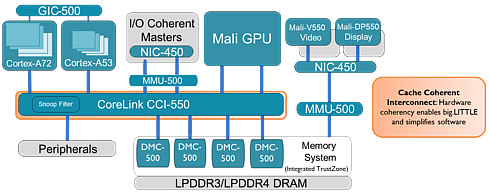
ARM says that its next-generation Mali IP codenamed "Mimir" will be fully cache-coherent and would be a perfect fit to take advantage of such a configuration. Fully coherent GPUs will be able to take advantage of shared virtual memory and new simplified programmers models provided by APIs such as OpenCL 2.0 and HSA.
| Feature |
CoreLink |
CoreLink |
CoreLink |
|---|---|---|---|
Summary |
Smallest area 2 cluster coherent interconnect |
Highly configurable ACE interconnect supporting up to 4 clusters |
Highest performance ACE interconnect supporting up to 6 clusters or mix of CPU and fully coherent GPU |
ACE Slave interfaces (fully coherent) |
2 |
1-4 |
1-6 |
ACE-Lite Slave interfaces (IO coherent) |
1-3 |
0-6 (maximum 7 ACE and ACE-Lite slave ports) |
0-6 (maximum 7 ACE and ACE-Lite slave ports) |
Memory and System master interfaces |
1-2 memory channels 1 system |
1-4 memory channels 1-2 system |
1-6 memory channels 1-3 system (maximum 7 ports) |
Memory Map |
40 bit Physical |
32-48 bit Physical, configurable address map 40/44/48 bit DVM |
|
Coherency and snoop filter |
Broadcast snoop coherency |
Integrated snoop filter maintains directory of processor cache contents and reduces CPU snoops |
|
Performance enhancements |
Higher frequency and interface count than CoreLink CCI-400 offering higher peak bandwidth |
Read data buffers (configurable) Up to 2x snoop data bandwidth (configurable) Supporting system bandwidths in excess of 50GB/s |
|
Power, area, frequency |
CoreLink CCI-500 and CCI-550 are capable of > 1 GHz clock on modern process technology |
||
The CoreLink DMC-500 memory controller provides higher bandwidth and latency response for processors and display.
CoreLink CCI-550 includes improvements in the microarchitecture to deliver higher peak throughput for demanding use cases and quality of service (QoS) enhancements that reduce latency by 20 percent. SoC designers can configure the number of memory channels, tracker sizes, snoop filter capacity and scale up to 6 fully coherent processor clusters. The scalability addresses a wide range of applications beyond mobile including digital TV, automotive and cost-efficient networking applications.
Time and energy-intensive memory transactions require a memory controller designed with a system approach to reduce bottlenecks. For ARM Cortex processors, CoreLink DMC-500 offers the lowest latency and power along with enhanced QoS for LPDDR4/3 memories operating up to LPDDR4-4267 transfer speeds. When integrated at the design level, CoreLink CCI-550 and CoreLink DMC-500 work together to deliver a peak system memory bandwidth beyond 50GB/s for access to richer content such as 4K video, with predictable performance.
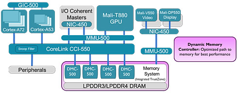
Performance CoreLink DMC-500
| |
LPDDR3 |
LPDDR4 |
|---|---|---|
Data Rate (per pin) |
800 ~ 2133 Mbps |
400 ~ 3200 Mbps (~4266Mbps) |
Density |
4Gb ~ 32Gb |
8Gb ~ 32Gb |
Interface |
HSUL_12 w/optional ODT |
LVSTL |
Command/Address Bus |
DDR |
SDR (Multi cycle command) |
Data Bus |
DDR |
DDR |
Voltage (VDD1 / 2 / CA / Q) |
1.8V / 1.2V / 1.2V / 1.2V |
1.8V / 1.1V / 1.1V |
I/O Organization |
X16 / x32 |
2 ch. X16 (total x32 per die) |
Number of Banks |
8 |
8 / ch. (total 16 banks per die) |
Pre-fetch |
8 |
16 |
Burst Length |
8 |
16 / 32 / On the fly |
CA ODT |
- |
Supported |
DQ ODT |
Supported (Optional) |
Supported |
On die ECC |
- |
For future DRAM process (vendor specific / transparent spec) |
Package Types |
MCP / PoP |
MCP / PoP |
| Product |
CoreLink DMC-500 |
|---|---|
System Interface |
AXI4 |
# SIs |
2 |
# Memory Channels |
1 |
LPDDR4/3 |
Yes |
Maximum DDR speeds |
X32 LPDDR3-2133, X16/X32 LPDDR4-4267 |
X32/X64 programmable support |
NA |
# Chip Selects (per channel) |
2 |
Both CoreLink products are available for licensing with production silicon expected by late 2016.

