NVIDIA Details GF100 GPU
Nvidia provided some details about the highly anticipated GF100 GPU, based on the new 'Fermi' architecture.
Scheduled for release sometime in April, the GF100 is comprised of four main units, Nvidia calls "Graphics Processing Clusters" or (GPC). Each GPC includes 4 "Streaming Multiprocessor cores" (SP), resulting to a total number of 16 SP.
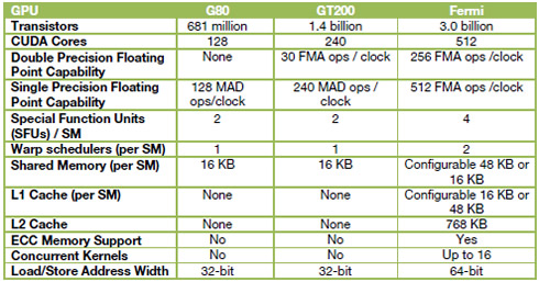
Each GPC also has a 'Raster Engine'. Nvidia claims that the GF100 has also dedicated hardware tessellators, or what Nvidia calls 'polymorph engines', appearing one per SM. Breaking this down further, each of the SMs comprise of 32 CUDA cores, 16 or 48KB of shared memory and 16 or 48KB of L1 cache and 4 texture units.
Basic features:
3 billion transistors
512 cores CUDA cores
16 Streaming Multiprocessors (SM)
16 Polymorph engines
4 Raster Engine Units 768KB L2 cache
64 Texture units
48 ROPs
384-bit memory interface (GDDR5)
A closer look at the following diagram could be helpful to understand the GF 100's main architecture:
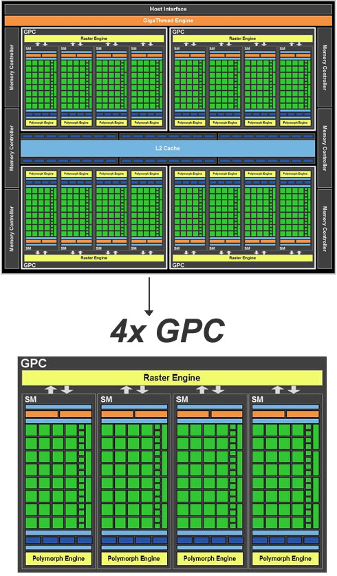
As you can see the GF100 looks more like a GPGPU chip rather than a GPU.
What about clock speeds, performance or power requirements? Nvidia has not provided any details. At CES2010, Nvidia showed off the tessellation capabilities pf the GF100 system using the Unigine Heaven benchmark. The company claimed that the GF100 beat the ATI 5870 by 60 percent. However, the company did not ran any synthetic benchmarks and also chose not to compare it with a comparably priced ATI HD5970 Hemlock card - which also supports tessellation.

Each GPC also has a 'Raster Engine'. Nvidia claims that the GF100 has also dedicated hardware tessellators, or what Nvidia calls 'polymorph engines', appearing one per SM. Breaking this down further, each of the SMs comprise of 32 CUDA cores, 16 or 48KB of shared memory and 16 or 48KB of L1 cache and 4 texture units.
Basic features:
3 billion transistors
512 cores CUDA cores
16 Streaming Multiprocessors (SM)
16 Polymorph engines
4 Raster Engine Units 768KB L2 cache
64 Texture units
48 ROPs
384-bit memory interface (GDDR5)
A closer look at the following diagram could be helpful to understand the GF 100's main architecture:

As you can see the GF100 looks more like a GPGPU chip rather than a GPU.
What about clock speeds, performance or power requirements? Nvidia has not provided any details. At CES2010, Nvidia showed off the tessellation capabilities pf the GF100 system using the Unigine Heaven benchmark. The company claimed that the GF100 beat the ATI 5870 by 60 percent. However, the company did not ran any synthetic benchmarks and also chose not to compare it with a comparably priced ATI HD5970 Hemlock card - which also supports tessellation.
