Samsung Completes 5nm EUV Development As it Races With TSMC
Samsung Electronics today announced that its 5-nanometer (nm) FinFET process technology is complete in its development and now is ready for customers’ samples.
Compared to 7nm, Samsung says its 5nm FinFET process technology provides up to a 25 percent increase in logic area efficiency with 20 percent lower power consumption or 10 percent higher performance. However, those gains mark a relatively minor advance. In October, Samsung said its 7LPP process would deliver up to a 40% shrink and up to 20% higher speeds or 50% lower power consumption compared to its 10nm node.
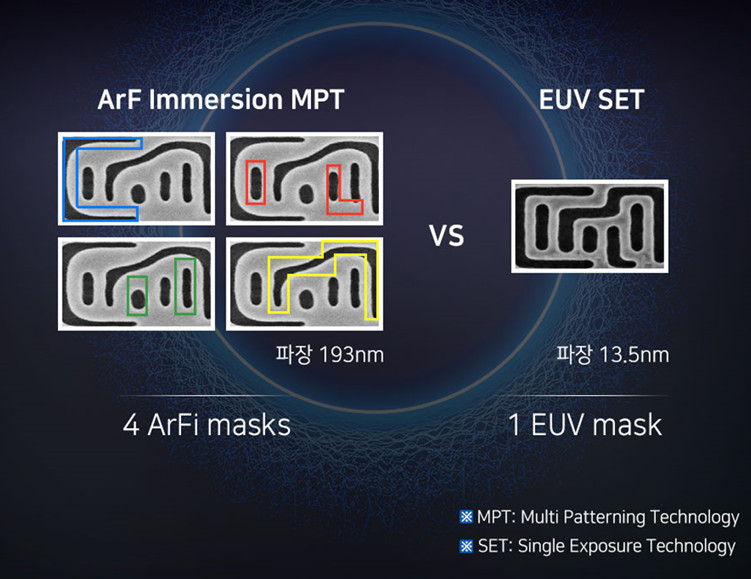
In addition to power performance area (PPA) improvements from 7nm to 5nm, Samsung's customers can leverage the EUV technology. Like its predecessor, 5nm uses EUV lithography in metal layer patterning and reduces mask layers while providing better fidelity.
Samsung says that 5nm will also feature new innovations including Samsung’s proprietary Smart Diffusion Break (SDB) transistor architecture.
The company declined to share line widths and pitches used on its 5nm node or relative costs of the new process.
“We’ve been using EUV on 7nm mostly in the back end, but for 5nm we are adding a little more [use of EUV] to the middle of the line,” said Shawn Han, a senior vice president for Samsung’s foundry group. “We are in a leadership position for EUV productivity,” he added, declining to share specifics about EUV wafer throughput, uptime or defect levels.
Another benefit of 5nm is that we can reuse all the 7nm intellectual property (IP) to 5nm. Thereby Samsung's 7nm customers’ transitioning to 5nm will benefit from reduced migration costs, pre-verified design ecosystem, and consequently shorten their 5nm product development.
In October 2018, Samsung announced the readiness and its initial production of 7nm process, its first process node with EUV lithography technology. The company has provided commercial samples of the EUV-based new products and has started mass production of 7nm process early this year.
In October, Samsung had also said it’s EUV throughput was at or above 1,500 wafers/day. It’s light source delivered a 250W sustained performance and a 280W peak, though it targeted 300W.
Also, Samsung is collaborating with customers on 6nm, a customized EUV-based process node, and says it has already received the product tape-out of its first 6nm chip.
TSMC responded to Samsung's announcement with its own 6-nanometer (N6) process, designed to offer a "competitive performance-to-cost advantage as well as fast time-to-market with direct migration from N7-based designs."
TSMC’s N6 process is leveraging the new capabilities in extreme ultraviolet lithography gained from the N7+ technology to deliver 18% higher logic density over the N7 process, according to TSMC. At the same time, its design rules are fully compatible with TSMC’sN7 technology.
TSMC’s N6 technology is scheduled for risk production in the first quarter of 2020.
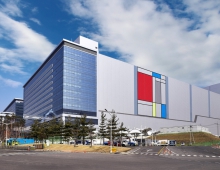
Samsung foundry’s EUV-based process technologies are currently being manufactured at the S3-line in Hwaseong, Korea. Additionally, Samsung will expand its EUV capacity to a new EUV line in Hwaseong, which is expected to be completed within the second half of 2019 and start production ramp-up from next year.

The South Korean company is now trying to attract customers who would use its new EUV-based 7-nm production line, which will go into full operation from 2020. It needs to secure enough orders from customers before the new line starts full operation. Major potential customers include Qualcomm, NVIDIA, IBM and Apple.
Previously, Apple used a multivendor strategy and placed orders on both TSMC and Samsung Electronics. Yet Apple has been relying exclusively on TSMC for production of its application processors starting from the iPhone 8. Apple is also facing a shortage of 5G modem chips due to its legal battle with Qualcomm, and Samsung has been mentioned as a candidate for Apple's 5G modem chip design and production.
Late last year, Samsung managed to win orders from IBM for production of high-performance CPUs for servers. IBM's order was largely due to the failure of GlobalFoundry, which has produced IBM's products, to develop a 7-nm EUV process.
Taiwan's TSMC, the No. 1 player in the global foundry market, has recently completed a system semiconductor design platform for its 5nm process. As TSMC has completed the process design platform, it is likely that the construction of the facility has also come close to comletion.
TSMC is already working to perfect the 5nm manufacturing process, although it is unknown when it goes into operation. Market analysts speculate that the new process could be used to producing Apple’s “A14” system-on-chip for the 2020 edition of the iPhones.
AMD, Apple, HiSilicon, Nvidia, Qualcomm and others are already collaborating with TSMC at 5nm. Samsung needs an edge over TSMC, and it also has to increase its packaging support for mobile applications.
Samsung Electronics said last year that it has completed the performance verification of a 3nm process and was working for technological perfection. The company is developing a technology in which a gate-all-around (GAA) transistor structure has been applied to a 3nm process.
GAA is a next-generation transistor structure that has been improved from the FinFET structure used in current semiconductor processing. Unlike FinFET, where the gate wraps around the three sides of the channel, the gates in GAA encloses all four sides of the channel, which allows the current flow to be controlled more precisely. Samsung explained that from the 3-nano process, it becomes a whole new level of microprocessing.