Samsung Develops Ultra-Thin Multi Chip Technology
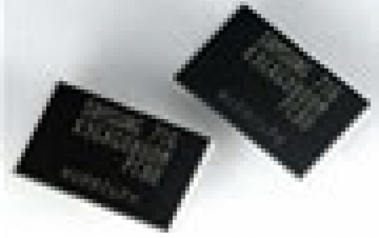
Samsung developed an 8-chip technology with a thickness of just 0.6mm, the world's thicknes multi-die package according to the company.
Multichip refers to the product that piles up single semiconductors to increase memory capacity and this is the first time to implement less than 1mm in thickness.
The new technology was applied to 32GB nand flash multi chip. The new 0.6mm-thick package, which consists of eight identical dies, uses 30nm-class, 32Gb NAND Flash chips, each measuring just 15?m, to deliver a 32GB NAND solution.
Existing nand flash multi chip package implemented only 1mm by processing wafer to 60?m. If process the thickness of wafer to below 30?m, it will be hard to maintain strength of chip and secure yield rate because gap between multi chips will become too narrow.
Samsung succeeded in overcoming technical limit to process wafer to 15?m. By securing processing technology, it will be able to pile more chips to increase capacity. This means that consumers can see thinner SSD and memory cards, for example.
Samsung claims that the 8 layer multichip with 0.6mm is the most suitable solution in mobile devices market. The new packaging technology is claimed to deliver a 40% thinner and lighter memory solutions for high-density multimedia handsets and other mobile devices.
In addition, the package technology can be adapted to other existing MCPs, configured as system in packages (SiP), or package on packages (PoP).
New Semiconductor R&D Center
In related news, Samsung today announced that its new Semiconductor Research & Development Center has started advanced logic process development. The Semiconductor R&D center brings together Samsung?s advanced logic and memory process research teams into one organization to realize synergies in various areas including new materials, transistor structures, and early access to leading edge process equipment.
Samsung Foundry, one of the key growth engines of Samsung Electronics, offers advanced logic process manufacturing to fabless and IDM companies. Currently in mass production at 45 nanometer (nm), Samsung is also preparing next generation 32-/28-nm and beyond process technologies through its continued participation in the IBM Technology Alliance.
The Semiconductor R&D center is focused on next generation semiconductor process development for both memory and logic applications, including sub-28nm process technology. At these advanced nodes, Samsung will leverage memory process development advancements to foundry logic process development and vice versa. Expected synergies include a broad spectrum of technologies including High-K, 3D transistors, and advanced lithography such as extreme ultra violet (EUV), which Samsung is a leader in. Additionally, Samsung?s Semiconductor R&D center is developing innovative interconnect and packaging solutions for these deep sub-micron technology nodes including through silicon via (TSV), where vertically stacked chips are connected with through silicon vias to enhance speed and performance.
The research efforts at this R&D center will complement other consortiums and joint development activities, including not only the IBM Technology Alliance, but also Samsung?s participation in IMEC and Sematech.


