Samsung Now Mass Producing First 2nd-Generation, 10-Nanometer Class DRAM
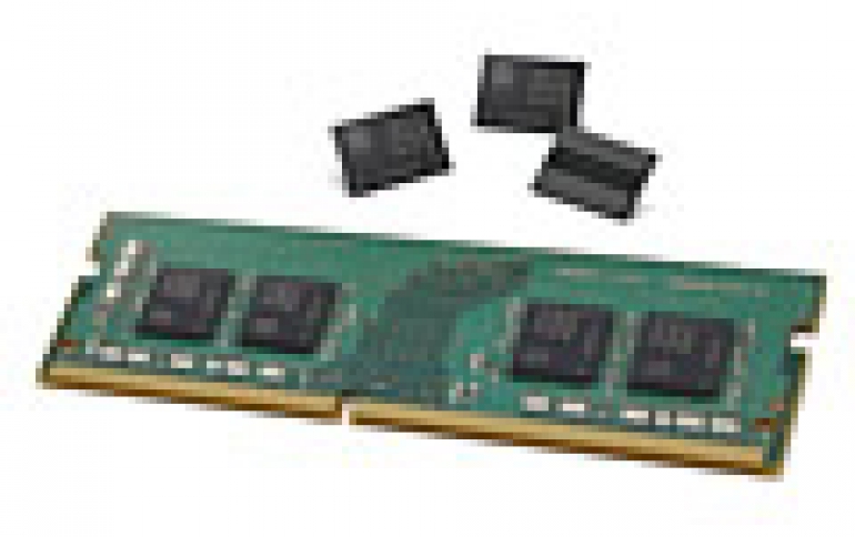
Samsung Electronics has begun mass producing the industry's first 2nd-generation of 10-nanometer class (1y-nm), 8-gigabit (Gb) DDR4 DRAM, The chips achieve speeds of up to 3,600 Mbps and are produced without the need for extreme ultraviolet (EUV) lithography.
Designed for use in a wide range of next-generation computing systems, the new 8Gb DDR4 features the highest performance and energy efficiency for an 8Gb DRAM chip, as well as the smallest dimensions.
"Through a rapid ramp-up of the 2nd-generation 10nm-class DRAM, we will expand our overall 10nm-class DRAM production more aggressively, in order to accommodate strong market demand and continue to strengthen our business competitiveness," said Gyoyoung Jin, president of Memory Business at Samsung Electronics.
Samsung's 2nd-generation 10nm-class 8Gb DDR4 features an approximate 30 percent productivity gain over the company's 1st-generation 10nm-class 8Gb DDR4. In addition, the new 8Gb DDR4's performance levels and energy efficiency have been improved about 10 and 15 percent respectively, thanks to the use of a proprietary circuit design technology. The new 8Gb DDR4 can operate at 3,600 megabits per second (Mbps) per pin, compared to 3,200 Mbps of the company's 1x-nm 8Gb DDR4.

To enable these achievements, Samsung has applied new technologies, without the use of an EUV process. The innovation here includes use of a high-sensitivity cell data sensing system and a progressive "air spacer" scheme.
In the cells of Samsung's 2nd-generation 10nm-class DRAM, a newly devised data sensing system enables a more accurate determination of the data stored in each cell, which leads to a significant increase in the level of circuit integration and manufacturing productivity.
The new 10nm-class DRAM also makes use of a unique air spacer that has been placed around its bit lines to dramatically decrease parasitic capacitance. Use of the air spacer enables not only a higher level of scaling, but also rapid cell operation.
With these advancements, Samsung is now accelerating its plans for much faster introductions of next-generation DRAM chips and systems, including DDR5, HBM3, LPDDR5 and GDDR6, for use in enterprise servers, mobile devices, supercomputers, HPC systems and high-speed graphics cards.
Samsung has finished validating its 2nd-generation 10nm-class DDR4 modules with CPU manufacturers, and next plans to work with its global IT customers in the development of more efficient next-generation computing systems.
In addition, the DRAM producer expects to not only rapidly increase the production volume of the 2nd-generation 10nm-class DRAM lineups, but also to manufacture more of its mainstream 1st-generation 10nm-class DRAM.
Samsung is planning to begin transitioning to EUV for logic chips next year at the 7nm node, although it is unclear when the technology will be put into production for DRAM. Because of the relative structural simplicity of DRAM cells, it is generally accepted that it will require EUV later than other types of devices.


