Samsung Starts Mass Producing First 10-Nanometer Class DRAM
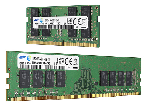
Samsung Electronics maintains its lead in advanced memory technology, as it has begun mass producing the first 18nm, 8-gigabit (Gb) DDR4 (double-data-rate-4) DRAM chips and the modules derived from them. Samsung says that it has managed to overcoming technical challenges in DRAM scaling. These challenges were mastered using currently available ArF (argon fluoride) immersion lithography, free from the use of EUV (extreme ultra violet) equipment.
According to thge company, key technology developments include improvements in proprietary cell design technology, QPT (quadruple patterning technology) lithography, and ultra-thin dielectric layer deposition.
Unlike NAND flash memory, in which a single cell consists of only a transistor, each DRAM cell requires a capacitor and a transistor that are linked together, usually with the capacitor being placed on top of the area where the transistor rests. In the case of the new 10nm-class DRAM, another level of difficulty is added because they have to stack very narrow cylinder-shaped capacitors that store large electric charges, on top of a few dozen nanometer-wide transistors, creating more than eight billion cells.
Samsung created the new 10nm-class cell structure by utilizing a proprietary circuit design technology and quadruple patterning lithography. Through quadruple patterning, which enables use of existing photolithography equipment, Samsung also built the core technological foundation for the development of the next-generation 10nm-class DRAM (1y).
In addition, the use of a refined dielectric layer deposition technology enabled further performance improvements in the new 10nm-class DRAM. Samsung engineers applied ultra-thin dielectric layers with "unprecedented uniformity" to a thickness of a mere single-digit angstrom (one 10 billionth of a meter) on cell capacitors, resulting in sufficient capacitance for higher cell performance.

Samsung's 18nm 8Gb DDR4 DRAM significantly improves the wafer productivity of 20nm 8Gb DDR4 DRAM by more than 30 percent.
The new DRAM supports a data transfer rate of 3,200 megabits per second (Mbps), which is more than 30 percent faster than the 2,400Mbps rate of 20nm DDR4 DRAM. Also, new modules produced from the 10nm-class DRAM chips consume 10 to 20 percent less power, compared to their 20nm-process-based equivalents, which will improve the design efficiency of high-performance computing (HPC) systems and other large enterprise networks, as well as being used for the PC and mainstream server markets.
Samsung's roll-out of the 10nm-class (1x) DRAM marks yet another milestone for the company after it first mass produced 20-nanometer (nm) 4Gb DDR3 DRAM in 2014.
Samsung expects to also introduce a 10nm-class mobile DRAM solution with high density and speed later this year.
Samsung's technological progress is expected to help the company cut the production costs sooner than its competitors, meaning that the company could further increase its profits.
Rival SK Hynix is currently increasing the proportion of early-end 20-nano process and is developing 1x-nano DRAM. It is also believed that Micron has yet to mass-produce early-end 20-nano DRAM.
It seems that the difference in technology between South Korean businesses and Micron is huge, with Micron to lag about 2 years behind.


