Breaking News

CASIO introduces a new limited edition Hammered heritage model, the New MRG-B5000HT Introducing the Game-Changing MINISFORUM G1 Pro PlayStation Plus Monthly Games for December 2025 SSSTC Launches 16TB Enterprise SATA SSD with Breakthrough IOPS Performance Lexar Unveils Industry’s First AI Storage Core for Next Generation Edge AI Devices

logo

  • Share Us
    • Facebook
    • Twitter
  • Home
  • Home
  • News
  • Reviews
  • Essays
  • Forum
  • Legacy
  • About
    • Submit News

    • Contact Us
    • Privacy

    • Promotion
    • Advertise

    • RSS Feed
    • Site Map

Search form

Samsung to Talk About 7nm SRAM EUV Design at ISSCC

Samsung to Talk About 7nm SRAM EUV Design at ISSCC

Enterprise & IT Nov 13,2017 0

Among the papers that will be presented at the International Solid-State Circuits Conference in February is one that describes how Samsung 7nm SRAM was made using extreme ultraviolet lithography (EUV).

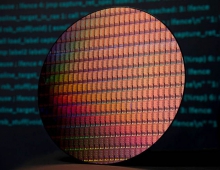
South Korean Samsung will describe a 0.026μm2 SRAM bit cell in a 7nm process it aims to make available next year. The chip is the smallest SRAM described to date and uses a double-write driver to reduce minimum supply voltage.

TSMC will describe an 11 Mbit resistive RAM macro made in a 40nm process. It uses a new sense amplifier TSMC claims offers a 58 percent faster access speed as well as a new write scheme to improve endurance and retention.

Both Samsung and SK Hynix will describe 16 and 8 Gbit GDDR6 DRAMs, respectively, with maximum data rates of 16-18Gbits/s/pin using single-ended signaling. SK Hynix also will detail its eight-layer HBM2 that delivers 64 Gbits of memory on a 341 GByte/s interconnect.

Samsung will present its Tbit NAND based on 64 stacked layers and four bits/cell. Toshiba and Western Digital will counter with a 512 Gbit design using three bits/cell in a 96-layer stack. Separately, Samsung will describe its Z-NAND that achieves a 15μs latency as well as a solid-state drive controller for it that aims to compete with Intel's Optane drives.

Separately, Sony will describe a 1.46MP BSI global shutter CMOS image sensor expected to be used for scientific and industrial applications. It employs an in-pixel ADC thanks to 3D stacking techniques.

Microsoft will present a 1024x1024 time-of-flight image sensor made in a TSMC 65nm process. Organizers said it sports the smallest pixels and highest resolution for such products routinely used in gaming, virtual reality, augmented reality and the Internet of Things.

TSMC will show a new architecture for a CMOS imager aimed to increase video frame rates four- to nine-fold. The 13.5MP 3D-stacked sensor uses a bank of column ADCs.

Google will present the concept of a single compute fabric for machine-learning from the device to the data center as well as the technical challenges to enable it.

The 2018 International Solid-State Circuits Conference will be held in San Francisco February 11-15, 2018.

Tags: EUV Lithography
Previous Post
New Servers Based on AMD EPYC and AMD Radeon Instinct Platforms Appear at SC17
Next Post
Qualcomm to Reject Broadcom's $103 billion Offer: reports

Related Posts

  • Samsung Expands its Foundry Capacity with A New 5nm Chip Production Line in Pyeongtaek, Korea

  • Samsung Announces First EUV DRAM with Shipment of First Million Modules

  • Imec and ASML Demonstrate 24nm Pitch Lines With Single Exposure EUV Lithography

  • Samsung Begins Mass Production at New EUV Manufacturing Line

  • Samsung Begins Volume Production of 6-nm Chips

  • U.S. Forced Dutch ASML to Cancel China Chip-equipment Sale

  • Future EUV to Move in Higher NA

  • Samsung Outlines Possible Solutions For EUV Process Challenges

Latest News

CASIO introduces a new limited edition Hammered heritage model, the New MRG-B5000HT
Consumer Electronics

CASIO introduces a new limited edition Hammered heritage model, the New MRG-B5000HT

Introducing the Game-Changing MINISFORUM G1 Pro
Enterprise & IT

Introducing the Game-Changing MINISFORUM G1 Pro

PlayStation Plus Monthly Games for December 2025
Gaming

PlayStation Plus Monthly Games for December 2025

SSSTC Launches 16TB Enterprise SATA SSD with Breakthrough IOPS Performance
Enterprise & IT

SSSTC Launches 16TB Enterprise SATA SSD with Breakthrough IOPS Performance

Lexar Unveils Industry’s First AI Storage Core for Next Generation Edge AI Devices
Enterprise & IT

Lexar Unveils Industry’s First AI Storage Core for Next Generation Edge AI Devices

Popular Reviews

be quiet! Dark Mount Keyboard

be quiet! Dark Mount Keyboard

Terramaster F8-SSD

Terramaster F8-SSD

be quiet! Light Mount Keyboard

be quiet! Light Mount Keyboard

Soundpeats Pop Clip

Soundpeats Pop Clip

Akaso 360 Action camera

Akaso 360 Action camera

Dragon Touch Digital Calendar

Dragon Touch Digital Calendar

Noctua NF-A12x25 G2 fans

Noctua NF-A12x25 G2 fans

be quiet! Pure Loop 3 280mm

be quiet! Pure Loop 3 280mm

Main menu

  • Home
  • News
  • Reviews
  • Essays
  • Forum
  • Legacy
  • About
    • Submit News

    • Contact Us
    • Privacy

    • Promotion
    • Advertise

    • RSS Feed
    • Site Map
  • About
  • Privacy
  • Contact Us
  • Promotional Opportunities @ CdrInfo.com
  • Advertise on out site
  • Submit your News to our site
  • RSS Feed