Samsung Talks About Process Technology Roadmap, Down to 3-nanometer Using GAA
The Samsung Foundry Forum 2018 Japan was held in Tokyo and Samsung disclosed details about its silicon innovations that will be at the heart of future high-performance computing and connected devices.
With process technology roadmap updates down to 3-nanometer (nm), Samsung Foundry is holding events worldwide focused on providing customers with the tools necessary to design and manufacture powerful, yet energy-efficient system-on-chips (SoC) for a wide range of applications.
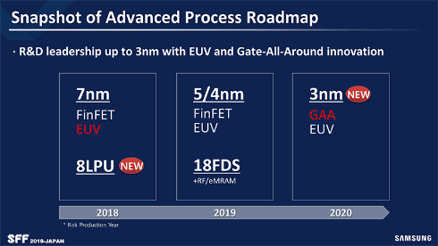
In the keynote speech of the forum, Samsung Foundry Division president Mr. ES Jung talked Samsung's "Gate-All-Around (GAA) 3nm process as well as the use of EUV (extreme ultraviolet) instead of the conventional ArF immersion in the next-generation chips.

7LPP, the first semiconductor process technology to use an EUV lithography solution, is scheduled to be ready for production in the second half of this year. Samsung said that key IPs were under development, aiming to be completed by the first half of 2019. This is an improved version of 8LPP (8nm Low Power Plus) of "8LPU", which will enter risk production this year.
5LPE (5nm Low Power Early) will succeed the 7LPP process, and will allow greater area scaling and ultra-low power benefits, according to Samsung.
The use of the mature and verified FinFET technology will also be extended to the 4nm process [4LPE/LPP (4nm Low Power Early/Plus)]. As the last generation of FinFET, 4nm provides a smaller cell size, improved performance, and faster ramp-up to the stable level of yield by adopting 5LPE, supporting easy migration.
At the same year, Samsung will also start risk production of 18 FD-SOI with eMRAM and RF capability
Finally, in 2010, Samsung plans to apply the 3nm process nodes, which will adopt GAA, the next-generation device architecture. To overcome the physical scaling and performance limitations of the FinFET architecture, Samsung is developing its GAA technology, MBCFET (Multi-Bridge-Channel FET) that uses a nano-sheet device. By enhancing the gate control, Samsung claims that the performance of 3nm nodes will be significantly improved.
Interestingly, Samsung said that the applications of chips made with the 7nm EUV process will include network, automotive, but not GPUs.
AMD plans to release its next-generation CPU "Zen 2" and the GPU architecture "Navi" this year, made using TSMC's 7nm process (immersion exposure). But considering that TSMC will also have to make 7nm SoCs for smartphone, it will be interesting to see whether there will be room in 7nm production line enough to cover GPU demands for NVIDIA and AMD.


