Samsung Wants to Lead the Foundry Race With Process Roadmap Down to 4nm
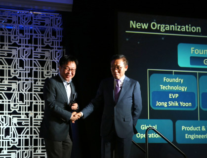
Samsung Electronics, the world's second-biggest chipmaker, is increasing its effort in semiconductor outsourcing by separating the company's foundry business into a new unit and announced a foundry process technology roadmap.
Specifically, Samsung aims to lead the industry with 8nm, 7nm, 6nm, 5nm, 4nm and 18nm FD-SOI in its newest process technology roadmap.
"The ubiquitous nature of smart, connected machines and everyday consumer devices signals the beginning of the next industrial revolution," said Jong Shik Yoon, Executive Vice President of the Foundry Business at Samsung Electronics. "To successfully compete in today's fast-paced business environment, our customers need a foundry partner with a comprehensive roadmap at the advanced process nodes to achieve their business goals and objectives."
Samsung's newest foundry process technologies and solutions introduced today at the annual Samsung Foundry Forum include:
- 8LPP (8nm Low Power Plus): Samsung says that the 8LPP provides the most competitive scaling benefit before transitioning to EUV (Extreme Ultra Violet) lithography - a new version of the process of burning the circuit patterns into layers of materials on silicon to create chips. Combining key process innovations from Samsung's 10nm technology, 8LPP offers additional benefits in the areas of performance and gate density as compared to 10LPP. 8LPP is coming later this year.
- 7LPP (7nm Low Power Plus): 7LPP will be the first semiconductor process technology to use an EUV lithography solution. Samsung says it has worked with ASML to develop 250W of maximum EUV source power, which is the most important milestone for EUV insertion into high volume production. EUV lithography deployment could break the barriers of Moore's law scaling, paving the way for single nanometer semiconductor technology generations. Samsung promises to apply 7LPP in 2018.
- 6LPP (6nm Low Power Plus): 6LPP will adopt Samsung's Smart Scaling solutions, which will be incorporated on top of the EUV-based 7LPP technology, allowing for greater area scaling and ultra-low power benefits.
- 5LPP (5nm Low Power Plus): 5LPP extends the physical scaling limit of FinFET structure by implementing "technology innovations" from the next process generation, 4LPP, Samsung said without providing further details.
- 4LPP (4nm Low Power Plus): 4LPP will be the first implementation of next generation device architecture - MBCFET structure (Multi Bridge Channel FET). MBCFET is Samsung's GAAFET (Gate All Around FET) technology that uses a Nanosheet device to overcome the physical scaling and performance limitations of the FinFET architecture. The company believes it will begin to introduce 4nm production in 2020.
- FD-SOI (Fully Depleted - Silicon on Insulator): Suited for IoT applications, Samsung will gradually expand its 28FDS technology into a broader platform offering by incorporating RF (Radio Frequency) and eMRAM(embedded Magnetic Random Access Memory) options. 18FDS is the next generation node on Samsung's FD-SOI roadmap with enhanced PPA (Power/Performance/Area).
The South Korean company on Wednesday also promised customers that it will have a new plant up and running by the fourth quarter of this year.
Creating a separate unit for the business may ease the concerns of some potential customers who compete with other parts of Samsung.

"As part of our commitment to play seriously in the foundry area we felt that it was best that we create an independent organization," said Kelvin Low, a senior director of foundry marketing. "That will result in less conflict of interest -- although that's not really an issue these days -- it's still a perception in some customers' minds."
Samsung's commitment underlines the importance of its chip unit and the growth in demand for outsourced production of chips. Currently, a few companies can afford to invest the billions of dollars it takes to build and equip plants and fund research into new manufacturing. TSMC, which dominates the market by producing components for companies such as Apple, has posted double-digit percentage revenue gains for the last five years.
In March, Intel, which is the world's largest maker of chips through its lead in the market for computer microprocessors, said it's recommitting itself to building its own made-to-order chip business and claimed its manufacturing is still ahead of Samsung and TSMC. All three companies fight for orders from companies such as Qualcomm and Apple, which design their own chips but don't own any manufacturing.
Currently the finest chip manufacturing process is 10-nanometer production. Samsung said it was the first to mass produce at that node and TSMC said it's now in full production of 10 nanometer with a rapid increase in output due in the second half of this year.


