Sony Commercializes Low-Power GNSS Receiver LSIs for Smartphones
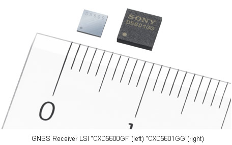
Sony today announced the commercialization of two Global Navigation Satellite System (GNSS) Receiver LSIs that consume just 10mW of power, and one GNSS Receiver Module for use in mobile products.
Sony will start offering the GNSS Receiver LSI "CXD5600GF" (¥1,000 / $10.7), "CXD5601GG" (¥1,500 / $16.07) GNSS receiver LSIs and the "CXD5430" GNSS receiver module (¥3,000 / $32.10 - includes flash memory and peripheral components) sequentially from June.
Location information is now widely used for purposes such as smartphone applications. However, this power-consuming functionality is shortening the battery life of mobile devices.
To overcome these challenge, Sony developed new RF and digital circuits featuring low-power AD converters, low noise amplifiers and electronic circuit phase-locked loops (PLL). Sony also adopted a low-power digital circuit design that optimally controls the power supply and clock for each separate function block. Conventionally, the power consumption of the RF circuits alone exceeds 10mW, but Sony claims it has successfully reduced power consumption to the industry's lowest 10mW for the entire GNSS Receiver LSI unit.

Furthermore, these LSIs are equipped with Sensor Fusion functionality, which facilitates arithmetic processing to measure highly accurate positional information by combining information received from multiple sensors built into the smartphone, such as accelerometers, magnetic sensors and gyro sensors. Even when indoors, or other environments where it can be difficult to measure a location with just the satellite signal reception, the technology is capable of generating autonomous navigation ('dead reckoning') to deliver highly precise positional information.
It is compatible with five measurement system, including the Global Positioning System (GPS), Global Navigation Satellite System (GLONASS), Quasi-Zenith Satellite System (QZSS) and satellite-based augmentation system (SBAS), as well as the Indoor Messaging System (IMES).
Sony plans to introduce these models in smartphones and tablets, as well as a wide variety of other products, including digital cameras, car navigation systems and wristwatches.
Location information is now widely used for purposes such as smartphone applications. However, this power-consuming functionality is shortening the battery life of mobile devices.
To overcome these challenge, Sony developed new RF and digital circuits featuring low-power AD converters, low noise amplifiers and electronic circuit phase-locked loops (PLL). Sony also adopted a low-power digital circuit design that optimally controls the power supply and clock for each separate function block. Conventionally, the power consumption of the RF circuits alone exceeds 10mW, but Sony claims it has successfully reduced power consumption to the industry's lowest 10mW for the entire GNSS Receiver LSI unit.

Furthermore, these LSIs are equipped with Sensor Fusion functionality, which facilitates arithmetic processing to measure highly accurate positional information by combining information received from multiple sensors built into the smartphone, such as accelerometers, magnetic sensors and gyro sensors. Even when indoors, or other environments where it can be difficult to measure a location with just the satellite signal reception, the technology is capable of generating autonomous navigation ('dead reckoning') to deliver highly precise positional information.
It is compatible with five measurement system, including the Global Positioning System (GPS), Global Navigation Satellite System (GLONASS), Quasi-Zenith Satellite System (QZSS) and satellite-based augmentation system (SBAS), as well as the Indoor Messaging System (IMES).
Sony plans to introduce these models in smartphones and tablets, as well as a wide variety of other products, including digital cameras, car navigation systems and wristwatches.
| CXD5600GF | CXD5601GG | CXD5430 | ||
|---|---|---|---|---|
| Compatible Satellite Systems | GPS, GLONASS, QZSS, SBAS, IMES | |||
| Hot Start Sensitivity | -163dBm | |||
| Tracking Sensitivity | -168dBm | |||
| Time To First Calculation | Less than 1sec. (at -145dBm) | |||
| Power Consumption |
Continuous Reception*2 | 10mW | 14mW | |
| Standby | Approx. 10μW | Approx. 10μW | ||
| Input Voltage | 1.8V - 3.3V | |||
| User Interface | UART, I2C | |||
| Other Functions | A-GPS support, Intermittent Tracking, Dead Reckoning, Noise Mitigation | |||
| Package | UFBGA-48Pin (WLCSP) |
VFBGA-56Pin (SiP) |
LLGA-35Pin (Module) |
|
| Size (length, width, height) | 2.9 x 3.0 x 0.6mm | 4.3 x 4.3 x 1.0mm | 9.8 x 7.5 x 1.5mm | |


