Toshiba Claims the world's Fastest Embedded DRAM Technology
Toshiba today announced that it has realized the world's fastest circuit technology for embedded DRAM for System LSI, achieving a speed of 833MHz at 32Mb density.
The technology will be applied to graphic processing LSI. The technology was today introduced at the ISSCC (International Solid State Circuits Conference), held at San Francisco CA from February 3rd.
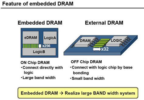
Embedded DRAM are applied to systems on chips for graphic application, as they can read larger data amounts at higher speeds than external memory. As video images achieve higher levels of definition, higher processing speeds of larger densities are required.

Toshiba applied a "pseudo two port system," a technology that virtually divides the overall memory into two and then reads and writes data in parallel and alternately. By replacing conventional serial read and write system with the new parallel technology, and optimizing such circuits as the command structure, Toshiba achieved the world's highest level of embedded DRAM performance ad 32Mb, a density actually applicable to products.
System LSI with embedded DRAM memory will find application in next generation high-end digital consumer products, game applications, mobile phones, projectors and other image-related applications that require high speed transfer of large volumes of data. Toshiba plans to apply this technology to its 65nm system LSI process, and to meet market demand for advanced graphic applications through the early launch of SoC integrating the new embedded DRAM.
Embedded DRAM are applied to systems on chips for graphic application, as they can read larger data amounts at higher speeds than external memory. As video images achieve higher levels of definition, higher processing speeds of larger densities are required.

Toshiba applied a "pseudo two port system," a technology that virtually divides the overall memory into two and then reads and writes data in parallel and alternately. By replacing conventional serial read and write system with the new parallel technology, and optimizing such circuits as the command structure, Toshiba achieved the world's highest level of embedded DRAM performance ad 32Mb, a density actually applicable to products.
System LSI with embedded DRAM memory will find application in next generation high-end digital consumer products, game applications, mobile phones, projectors and other image-related applications that require high speed transfer of large volumes of data. Toshiba plans to apply this technology to its 65nm system LSI process, and to meet market demand for advanced graphic applications through the early launch of SoC integrating the new embedded DRAM.


