Intel-Micron 3D NAND To Have 32 Layers, 256Gb Per Die
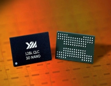
Intel will release its first 3D NAND flash chips solid-state drives next year and claims that it will manage to offer twice the density of competing products on the market now. 3D NAND moves focus away from miniaturization, which has traditionally focused on shrinking NAND cells. Instead, the shift will be toward increasing density via layering. While conventional memory chips basically consist of one layer of memory elements, 3-D chips are made by stacking up dozens of thin layers of memory elements. This multiple-layer method helps expand memory capacity dramatically.
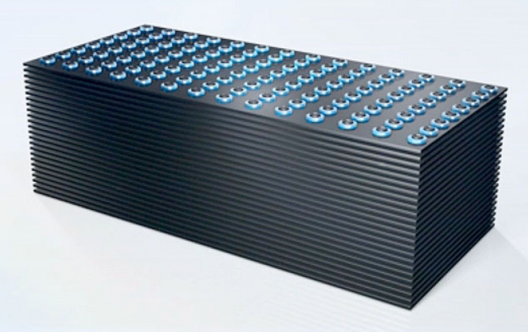
During an investor webcast, Rob Crooke, senior VP and general manager of Intel's non-volatile memory group, said that Intel's 3D NAND stacks 32 planar layers to deliver 256Gb (32GB) of storage in a single MLC die. The 3D NAND can also be packed with three bits per cell to hit 384Gb (48GB) per die. The new 3D NAND will enable 10TB SSDs "within the next couple of years," he said. The technology can also squeeze 1TB of storage into a form factor just two millimeters thick -- in an SSD that fits in your pocket.
Intel’s 3D NAND could deliver high performance and remain cost effective. Just one 4-inch server rack of Intel SSDs can deliver 11 million IOPS (input/output operations per second). For comparison, you would need a rack of hard disk drives measuring 500 feet tall to churn out the same performance. Beyond the savings in the cost of the drives, ther are also savings in power and cooling.
However, Crooke did not provide technical details relate to the manufacturing of such a dense 3D NAND and how Intel would overcome issues related to stacking the memory cell layers. He just said that Intel's long history of microchip manufacturing innovation allowed the company to overcome the challenge of drilling 4 billion holes in a silicon chip.
But he characterized the 3D tech as having a "breakthrough cost" and hinted that Intel will not work alone here and will only bring production in-house "if it makes sense."
Intel and Micron (IM Flash Technologies) plan to produce the new multi-level cell (MLC) flash chips with products available in the second half of 2015.
Samsung is already shipping SSDs made with 32-layer flash, but its products have half the bits per single TLC die.Toshiba is also trying to catch up with Samsung in the 3D NAND memory business. The Japanese company started to mass-produce products using 15nm process technology in April 2014 and is planning to shift to the products during the period from 2014 to 2015. Toshiba's next step is to will shift to its own 3D-NAND Flash technology, known as BiCS. The goal for the company is to achieve a lower production cost of BiCS products compared to that of 15nm-process products. Toshiba aims to stack much more than 30 memory cell layers but doubling the current throughput will take at least a year from now.
Observers say that both Toshiba and Samsung are looking to achieve 48 layers in 2015.


