IBM And Samsung Researchers Demonstrate ST-MRAM Scalability at 11nm
On the 20th anniversary of its invention at IBM Research, fabled nonvolatile "universal" magnetic random access memory (MRAM) is getting an upgrade. IBM announced that in collaboration with Samsung, it is using a spin-transfer torque (STT) design on its MRAM. Today, there are three main ways to store digital information, or bits, in the forms of "0’s" and "1’s": hard disk drives (HDD), dynamic random access memory (DRAM), and flash memory.
HDDs, invented by IBM in the 1950s, continue to be attractive for PCs and data centers due to their low-cost. But these devices are intrinsically slower, require quite a bit of power, and due to their mechanical moving parts, are less reliable.
In 1967, IBM Fellow Robert Dennard filed a patent for his world-changing invention known as DRAM. Decades later it remains a veritable workhorse, driving almost all computing devices today. Its main drawback is that it’s volatile, meaning when the device shuts off power, DRAM loses the data.
Today’s top non-volatile memory technology (retains data without the need for continued power) is flash. It is much faster at reading and writing data compared to HDDs, but is a laggard compared to DRAM. It also has an endurance problem, eventually breaking down after several thousand rewrite cycles.
For two decades, IBM scientists have been investigating several non-volatile memory devices including magnetoresistive random-access memory or MRAM, which uses the spin of an electron to store bits.
MRAM is based on a grid of cells with two ferromagnetic layers, separated by a thin insulating layer. When the two magnets are both pointing north, this corresponds to a "0". If the second magnet points south, they store a "1".
The first generation of MRAM, called field-switched MRAM, was written by applying large currents to generate magnetic fields to switch the second magnet between north and south. However, IBM scientist John Slonczewski saw a better way.
When a current is passed through the cell, the electrons transfer their spin from one magnet to the other and thereby switch the second magnet from north to south, or vice versa, thus writing the cell.
When introducing this invention in his 1996 paper, Slonczewski coined the term "spin transfer" torque to describe this new switching mechanism. This new generation of MRAM is called Spin Transfer Torque MRAM (often shortened to Spin Torque MRAM or STT-MRAM).
While first generation field-switched MRAM has been produced for years, technical challenges including lowering the write current prevented it from being scalable to high densities and thus wider adoption. Slonczewski’s invention opened up the possibility of using much smaller write currents, and hence much smaller write transistors, thus enabling much denser MRAM. However, to realize its full potential, a breakthrough in materials would still be required.
Inspired by Slonczewski, scientists around the world, including teams at IBM and Samsung, continued to believe in the promise of MRAM because it offers several distinct advantages. MRAM is a memory (or indeed emerging memory) that combines unlimited endurance (read and write cycles), with inherent non-volatility.
This combination makes MRAM a great potential technology for always-on devices such as Internet of Things sensors, mobile devices and wearable electronics, offering more storage and longer battery life. In addition, since MRAM uses standard transistors, and is compact and robust, it’s more easily embedded on the same chip as logic and other functions, compared to flash memory. Therefore many semiconductor foundries are considering replacing embedded flash with embedded Spin Torque MRAM at the 28 nm node and beyond.
"With these capabilities a single MRAM chip can replace a combination of SRAM and flash for many ultra-low power, medium performance mobile and Internet of Things applications. However, our long term goal remains to scale Spin Torque MRAM to be so dense and fast it can be used as a cache memory in IBM’s servers," said Dr. Daniel Worledge, a scientist and MRAM team senior manager at IBM Research.
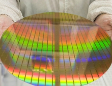
Appearing today in IEEE Magnetic Letters, Worledge and his IBM colleagues and partners at Samsung have published a paper demonstrating switching MRAM cells for devices with diameters ranging from 50 down to 11 nanometers in only 10 nanoseconds, using only 7.5 microamperes - a significant achievement.
"With PMA we are capable of delivering good STT-MRAM performance down to 7x10⁻¹⁰ write-error-rate with 10 nanosecond pulses using switching currents of only 7.5 microampere. This could never be done with in-plane magnetized devices - they just don’t scale. While more research needs to be done, this should give the industry the confidence it needs to move forward. The time for Spin Torque MRAM is now," said Worledge.
"In the 20 years since these scientific discoveries at IBM Research and elsewhere, the phenomenon of spin transfer torque has inspired significant research and development effort. These have now led to an STT switched magnetic memory device of 11 nm in size, back-end integrated onto CMOS circuits. This advance brings more possibilities to applications, and will accelerate the pace of innovation in the solid-state memory technology space," said Jonathan Sun, a research staff member on Worledge’s team.