Mitsui Chemicals to Provide ASML With Mask Protection Pellicles for EUV
Mitsui Chemicals, Inc. has signed a license agreement for the EUV pellicle business with ASML, the global No.1 company in the field of semiconductor lithography systems.
ASML is the only manufacturer which has successfully developed EUV pellicles for commercial use in its EUV lithography systems. The license agreement will bring synergy between ASML’s technology of EUV pellicle and Mitsui Chemicals’ long term track record in the pellicle business since its launch in 1984. The collaboration will contribute to the adoption of EUV lithography technology through the supply of high quality EUV pellicles in high volume, to support the growing demand in the market.
Based on this agreement, Mitsui Chemicals will start building an EUV pellicle assembly factory at Iwakuni Otake Works with a target schedule of completion by the 2nd quarter of 2020. After a ramp up period, Mitsui Chemicals aims for starting sales of EUV pellicle to customers by the 2nd quarter of 2021.
Mitsui Chemicals, as an established pellicle supplier, will be the 1st pellicle manufacturer to commercialize EUV pellicles conform ASML’s technology. Under the license agreement, ASML will continue to develop the EUV pellicle technology.
Lithography is the microfabrication technology that uses laser light for the production of Integrated Circuit (IC) and Liquid Crystal Display (LCD). The light is projected using a photomask (also known as a reticle) that contains the pattern of a circuit/device that will be printed onto a wafer. A lens or mirror focuses the pattern onto the wafer - a thin, round slice of semiconductor material - which is coated with a light-sensitive material (photo resist).
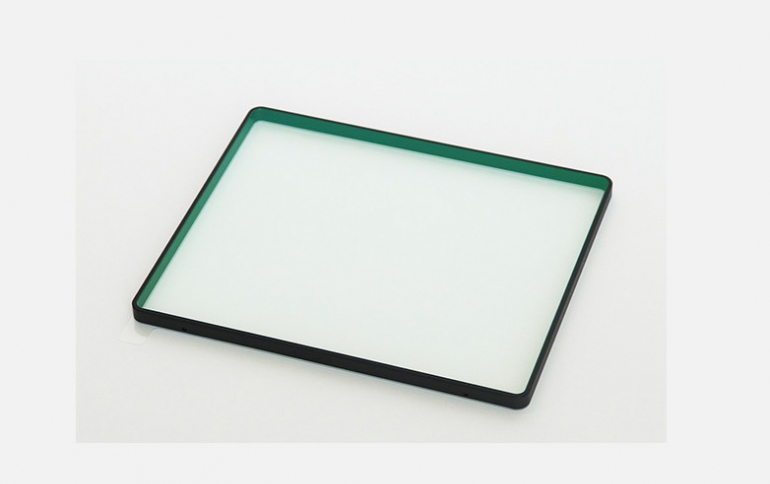
Pellicle is a dust-proof cover that protects the photomask pattern from foreign materials and contributes to the productivity improvement of semiconductor manufacturing, especially for the production of ultrafine semiconductors below the 7 nm. The pellicle helps to prevent foreign materials from being printed onto semiconductor wafers.
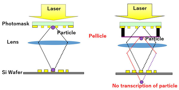
Unlike conventional argon fluoride (ArF), an EUV pellicle must be designed for a structure that reflects the light source several times to reach the wafer. The light must be suitable to compensate for the loss generated through the multilayer thin film special mirror. It should be made into ultra-thin film with a thickness of 50 nm and a size of 110 mm and 144 mm.
The EUV pellicle is an expensive product with prices ranging from 2,000 to 30 million won."
In South Korea, FST and S&E Tech are also developing EUV pellicles.

