Cadence Announces New Memory Standard Support in Samsung Foundry’s Advanced Process Technologies
Cadence Design Systems, Inc. supports the memory technologies across a range of Samsung Foundry's advanced process technologies targeting high-bandwidth applications.
Cadence has taped out DDR5/4 PHY IP on the Samsung 7nm Low Power Plus (7LPP) process, GDDR6 PHY IP on the Samsung 14nm Low Power Plus (14LPP) process and 2.4G High-Bandwidth Memory 2 (HBM2) PHY IP on the Samsung 10nm Low Power Plus (10LPP) process, which has been recharacterized as the 8nm Low Power Plus (8LPP) process. In addition, Cadence PHY IP for GDDR6 has achieved silicon success on the Samsung 7LPP process. Cadence says that Samsung's customers can begin creating designs using the foundry’s advanced process technologies and the Cadence DRAM interface IP.
The Cadence IP that supports Samsung Foundry’s various advanced nodes is intended for several emerging application areas including high-performance computing (HPC), mobile, artificial intelligence (AI), IoT, graphics, automated driving (AD) and adaptive driver assistance systems (ADAS).
Cadence offers:
- Design techniques reuse technology from Cadence’s DDR and SerDes designs, resulting in lower risk when implementing advanced memory technologies
- Cadence’s low bit-error rate (BER) for GDDR6 IP reduces retries on the memory bus, giving applications greater bandwidth and lower maximum latency
- Cadence’s design margin allows users to implement GDDR6 on PCBs using normal fiberglass FR4 materials, reducing the cost of GDDR6 deployment
- Cadence’s reference design for memory interfaces allows users to replicate Cadence’s test chip results in their own products
- Cadence DRAM controllers are based on the industry-leading Denali® DDR controller, which includes a full set of features for popular memory interfaces
Samsung’s advanced nodes and the Cadence IP offers the following performance specifications:
- GDDR6 technology using Cadence IP allows up to 512Gbit/sec between the host CPU and a single GDDR6 die
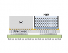
- HBM2 technology using Cadence IP allows up to 2400Gbit/sec bandwidth between host CPU and a single stack of HBM2
- DDR5 technology using Cadence IP allows up to 128Gbytes of DRAM per channel
Cadence PHY IP for GDDR6, DDR5/4 and HBM2, as well as memory models, are available now for the company's customer engagements. Design files are also ready for select customers to begin integration work.

