Hitachi Says It Has Developed World's Smallest IC Chip
Hitachi said Monday it has developed the world's thinnest intergrated circuit (IC) chip, which can be embedded in paper to track down parcels or prove the authenticity of a document.
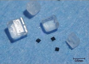
The IC chip is as small as a speck of dust, being just 0.15 mm by 0.15 mm square by 7.5 micrometers thick. The chip is a smaller version of the 0.4 x 0.4 mm "μ-Chip" currently being marketed by Hitachi. The distance between each circuit element was reduced by using SOI technology. In the conventional fabrication process, a transistor is formed directly upon the silicon substrate. In the SOI process, an insulation layer and a monocrystalline silicon layer (referred to as silicon on insulator) is formed upon the base silicon substrate, and the transistor is formed on this SOI substrate. Parasitic capacitance and leakage current are significantly reduced compared to the conventional process, and therefore transistor performance is increased.

Compared to the 0.3 x 0.3 mm, 60μm thick IC chip (henceforth 0.3mm IC chip) announced by Hitachi in February 2003, surface area is reduced to a quarter of the original size. Developments in thin chip fabrication technology have also enabled the chip to be reduced to one-eighth the thickness of the 0.3mm IC chip, at the same time. This significant decrease in size, increases the number of chips which can be fabricated on a single wafer, thus increasing productivity by more than four times.
The μ-Chip also uses an external antenna to receive radio waves (2.45 GHz microwaves), and transforms it to energy to wirelessly transmit a 128 bit (1038) unique ID number. As the data is written during the fabrication process using ROM (Read-Only-Memory) and thus provides a high level of authenticity.
The μ-Chip may be utilized in a broad range of applications such as security, transportation, amusement, traceability and logistics.


