Huawei P30 Pro Teardown Shows Triple PCB, Sony Camera Tech
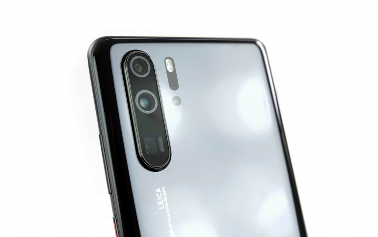
A teardown of Huawei's brand new P30 Pro smartphone by iFixit unveils the secrets of the device's Leica "quad" rear camera system, multi-layered PCBs and more.
Let's take a glance of the smartphone's basic specs:
- 6.47" OLED display with FHD+ (2340 × 1080) resolution
- 8-core Huawei Kirin 980 Processor with dual neural-network processing units and Mali-G76 MP10 GPU
- 6 GB RAM and 128 GB onboard storage (configurable to 8 GB RAM and up to 512 GB storage)
- Leica "quad" rear camera with 40 MP wide-angle (ƒ/1.6 with OIS) + 20 MP ultra-wide angle (ƒ/2.2) + 8 MP telephoto (ƒ/3.4 with OIS) + Huawei time-of-flight module—plus, a 32 MP selfie cam (ƒ/2.0)
- A new earpiece speaker technology called "Acoustic Display Technology," plus an in-display fingerprint sensor
- USB-C charging port (but no headphone jack)
- IP68 water/dust-resistance rating
One of the most interesting features of the new device is its quad camera system, which includes a main camera, plus cameras for wide-angle, Time-of-Flight and a periscope view. All four use Sony CMOS image sensors.
The periscope camera capable of 10X zoom and claims no loss in image quality, while the smartphone does not need to use a long-barrel telescopic lens. The module is rotated 90° from the aperture, laying flat in the phone with a prism refracting the light onto the sensor. Huawei placed a CMOS image sensor vertically and put a mirror angled at 45 degrees at the back to increase the optical path. Sunny Optical Technology in China is said to have put the module together, using IP from Corephotonics in Israel. According to iFixit, this module isn't used between 1x-5x zoom, coming into play beyond 5x zoom only.
Sony Time-of-Flight camera -- already used by Oppo -- coupled with a flood illuminator is used to enable AR functionality but also for “Auto focus." By processing signals from all three cameras, the ToF camera helps map out a scene and allow a user to focus on a specific object.
The dual-camera module uses a filter consisting of RYYB (Red, Yellow, Yellow, Blue) instead of usual RBG. While the main camera’s image sensor supplies RGB signals, the RYYB filter helps to bring in more light. This pattern is said to increase light sensitivity, and could help with contrast since they ditched the monochrome sensor from last year's P20 Pro.
The smartphone's motherboard comes in multiple stacks. Besides having multi-layered PCBs, this motherboard is actually two PCBs stacked on top of each other. Apple was the first smartphone vendor to do three-layer PCB in the iPhone X and Samsung followed suit, but Huawei is now following the trend. It turns out Huawei has used SLB (Substrate Like-PCB) assembly from Taiwan-based PCB supplier Unimicron.
In the P30 Pro, the bottom layer embeds Huawei’s chip division HiSilicon-developed Kirin applications processor, power management ICs and passive. All RF components occupy the top layer. In between, a mid-frame PCB connects the two and serves as an isolation layer.
The main board uses three pieces of PCB manufactured and assembled by Unimicron. The first PCB has the application processor and the power management ICs and passives. The second is a single-side PCB with all the RF components. Between these two pieces, a mid-frame PCB is use to make the connections.
Apple, in its iPhone X, placed memory on the top layer and an application processor in the middle layer. The third layer, providing thermal dissipation, was left blank.
A stacked PCB architecture enables the development of a substrate-like PCB with thick copper lines, meaning no loss in power and latency, while saving space.
The teardown also unveiled:
- SKhynix H9HKNNNFBMAU LPDDR4X—with the Huawei Kirin 980 layered underneath
- Micron JZ064 MTFC128GAOANAM-WT 128 GB flash storage
- HiSilicon HI6405
- HiSilicon HI6363 GFCV100 RF transceiver
- Skyworks 78191-11 low-band front-end module for WCDMA/LTE
- Qorvo 77031 mid/high-band front-end module front end module


