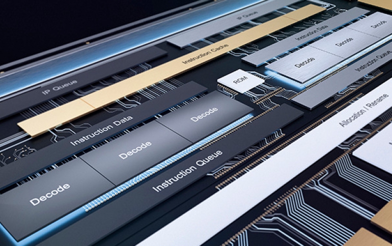
Intel Introduces the 10nm Atom Tremont Microarchitecture
Today at the Linley Fall Processor Conference in Santa Clara, Calif., Intel revealed the first architectural details related to Tremont.
Intel’s newest and most advanced low-power x86 CPU architecture, the 10nm Tremont low-power x86 microarchitecture delivers significant IPC (instructions per cycle) gains gen-over-gen compared with Intel’s prior low-power x86 architectures.

Intel's 10nm architecture begins with a focus on single-threaded performance but also brings other improvements, like the addition of L3 cache, a first for Atom, new power management enhancements that complement improved performance-per-watt, bolstered security, and support for new instructions.
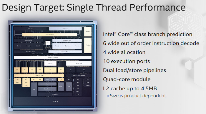
Intel says the culmination of these efforts results in up to 30% more IPC (at ISO frequencies) for Tremont compared to the previous-gen Goldmont Plus architecture (SPEC).
Using Intel’s 3D packaging technology Foveros, Tremont is integrated within a wider set of silicon IPs in Lakefield, which will powerdevices like the recently announced dual-screen Microsoft Surface Neo.
This approach allows Intel to meld together two different architectures to capitalize on the low-power and efficiency of the Tremont Atom cores and the high performance of the Sunny Cove core, bringing the two together in a combination similar to an ARM big.LITTLE processor, which Intel calls a "hybrid x86 architecture".
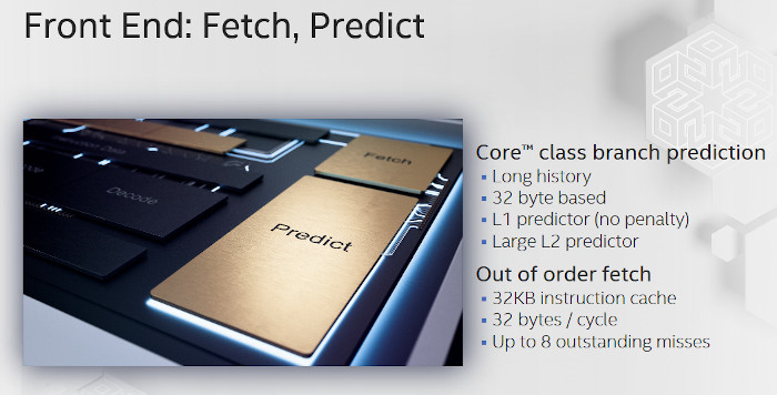
Getting into some technical details, Intel says it improved Tremont's branch predictor, saying that the Atom cores will have nearly the same accuracy as their high-power Sunny Cove Core family counterparts. This is accomplished with a new dual-stage branch prediction implementation. Intel states that there is no penalty for an L1 prediction, and that the L2 prediction penalty is smaller than previous generations.
The company also says that Tremont’s 6-wide (2×3-wide clustered) out-of-order decoder in the front end allows for a more efficient feed to the wider back end, which is fundamental for performance.
Another improvement for Intel after the decode engines is the re-order buffer. Intel states that it can support 208 instructions.

The chips will come with four-core modules that share an L2 cache that can be up to 4.5MB, but will vary based on specific products.
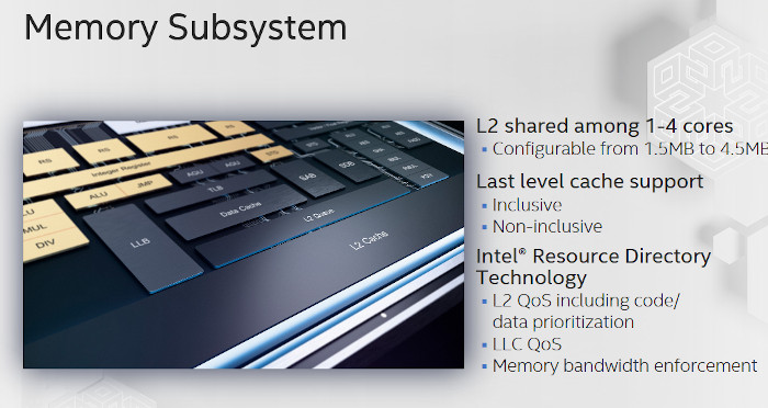
Intel has also increased the size of its L1 data cache. Both the L1-I and L1-D are now a 32 KiB/core design with 8-way associativity. Intel states that its L1 data cache here has a 3-cycle latency, compared to Skylake which has a 32 KiB L1D at a 4-cycle latency, or Sunny Cove which has a 48 KiB L1D at a 5-cycle latency.
Intel states that the L2 cache has an average 17-cycle latency.
Tremont also adds support for a global L3 cache across modules. Both the L2 and L3 cache support QoS arrangements, allowing for data prioritization and memory bandwidth enforcement for specific threads or virtual machines.

On the integer side, aside from the two AGUs, Tremont has 3 ALUs, a jump port, and a store data port. Each ALU supports different functions, with one enabling shift functions and another for multiplication and division. Compared to core, these ALUs are extremely lightweight, according to Intel.
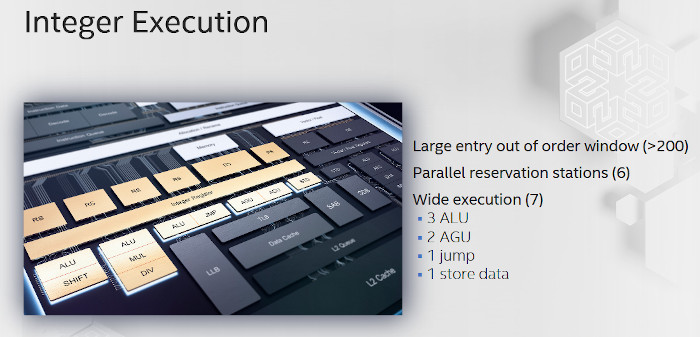
Intel has also made to the integer and vector units. The architecture features a larger 208-entry out of order window to accommodate the increased width, which in turn maximizes parallelism to the execution units. Six reservation stations feed the three ALU, two AGU (address generation unit), jump, and store ports.
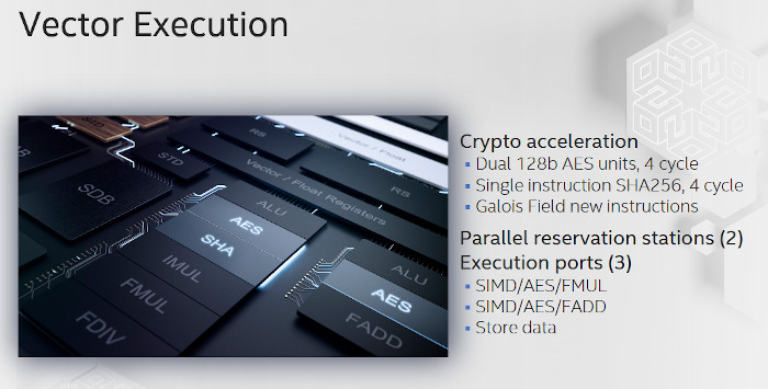
In addition, Intel improved crypto-acceleration in the vector unit by integrating dual 128-bit AES units with a four cycle latency, and a single-instruction SHA256 support with a four cycle latency, along with support for new Galois Field instructions.
Intel is moving Core down in power to the 1.5W level, and it will be interesting to see how Tremont can play in that 2mW to 2W range that Atom has traditionally played in.

