
Pulstec Showcases NEO-Series Nano Fabrication System at nano tech 2010
Pulstec, a company mostly known for its R&D on electronics, mechanics, opto-electronics and software, will showcase the NEO-series nano fabrication system at nano tech 2010 exhibition.
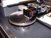 The NEO-500 Nanofabrication system, has been developed with National Institute of Advanced Industrial Science and
Technologies based on thermal lithography method
combined laser lithography method and thermal non-linear
material. The system can fabricate nano-scale structure on the
wide-area with low-cost and high-speed. The size of the
system is desktop type and can be used in the laboratory.
The system is capable of writing nano-scale structures at high speed directly on to the surface of a resist coated substrate (examples of typical substrates include semiconductor wafers or glass). The substrates are rotated in normal air condition. Compared to conventional lithography systems the NEO-500 has advantages of compact size and low investment costs without comprising performance, according to Pulstec. These advantages are achieved by using a visible semiconductor laser as a light source and Pulstec's uniquely designed optics.
The system can create continuous or periodic nano dot patterns and nano-scale grating. Application examples include optical filters, antireflective structures, photonic crystals, nano-imprint molding and biotechnology.
Held in Feb. 17 - Feb. 19 at Tokyo Big Sight, Japan, the nano tech 2010 International Nanotechnology Exhibition & Conference is the world's largest nanotechnology exhibition.


