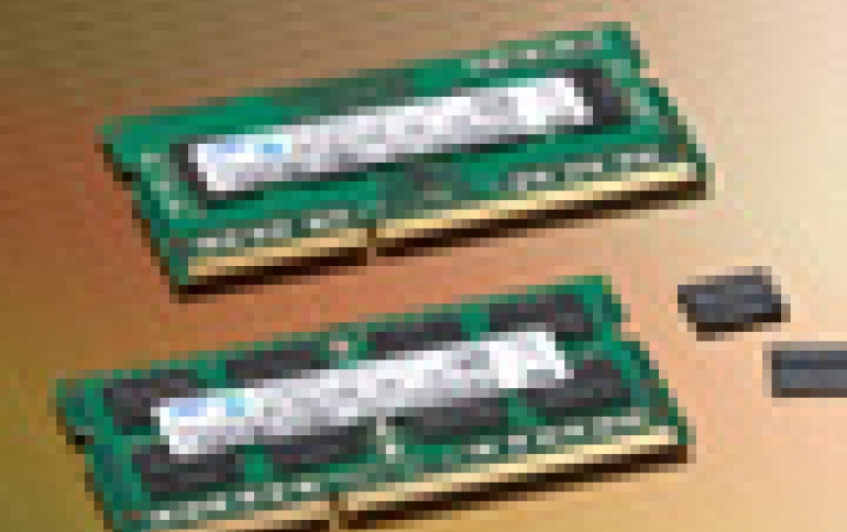
Samsung Begins Operation of World's Largest Memory Fab, Initiates Mass Production of 20nm-Class DDR3
Samsung announced today that it has begun operations of its new Line-16 memory semiconductor fabrication facility, which will provide the industry's largest production capacity.
The company also announced the start of mass production of double data
rate-3 (DDR3) dynamic random access memory (DRAM) based on 20 nanometer
(nm) class process technology, which offers significant improvements to
productivity and reduces energy consumption. The announcements were made
during a ceremony at Samsung's Nano City Complex in Hwaseong, Gyeonggi
Province, where the new Line-16 is located.
Receiving the first wafer from the new memory line, Samsung Electronics Chairman Kun-hee Lee said : "The global semiconductor industry is in a period of fierce cyclical volatility, so the opening of this new memory fab and the start of mass production of the world's first 20nm-class DRAM are important milestones to reinforce Samsung's industry leadership."
"We must prepare for an intensifying storm in the semiconductor industry by further enhancing our technological capabilities and expertise in order to maintain our leadership position," he said.
With the start of production at the new fab, which will constitute a total investment of 12 trillion Korean won through completion, Samsung aims to reinforce its leadership in the global memory semiconductor segment.
Samsung began construction of Line-16 in May 2010 and completed installation of equipment for clean rooms this May. Trial production began in June and the facility was made operational for mass production in August.
Housed in a 12-story building, Line-16 is the industry's most advanced and largest memory fabrication facility, with a combined workspace of approximately 198,000 square meters.
Starting this month, Samsung began mass production of high-performance 20nm-class NAND flash memory chips, with a projected volume of more than 10,000 12-inch wafers monthly.
Samsung plans to ramp up production of NAND flash memory to meet market demand, and will begin production of more advanced memory semiconductors with high density and performance using 10nm-class process technology next year.
Samsung also announced the mass production of 20nm-class 2 gigabit (Gb) DDR3 DRAM.
The 20nm-class DDR3 DRAM promises the most advanced performance yet, a further improvement on the 30nm-class DDR3 DRAM that Samsung introduced in July last year. The 20nm-class solution improves productivity by 50 percent and reduces energy consumption by up to 40 percent, therein providing the greenest DDR3 solution available.
With plans to also develop a new 20nm-class DDR3 component in 4Gb density by the end of 2011, Samsung will broaden its memory product lineup with mass production of 4 gigabyte (GB), 8GB, 16GB and 32GB DDR3 modules next year.
The world's second largest semiconductor maker Hynix hopes to develop 20-nanometer chips by the end of the year and begin production early next year. Japan's Elpida Memory said today that it would start mass production of a 25nm 4-gigabit DDR3 SDRAM by the end of this year.
Elpida's newly developed 4-gigabit DRAM enhances productivity by about 45% compared with Elpida's 30nm 4-gigabit DDR3 SDRAM. Compared with this same 30nm DDR3, it reduces operating current by about 25-30% and standby current by about 30-50%. It has also realized the industry's highest speed data transfer rate.


