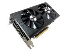
Sapphire X800
3. A closer look
The Sapphire X800 is built on the same fire red PCB we're used to seeing. However, one thing has definitely changed is the length of the board. The X800, just like the X800XL, is almost as long as the motherboard itself.
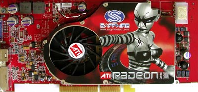 |
| The front side of the card.(click for hi-res). |
The metal plate located on the rear of the card serves two purposes. One is to hold the X800's cooler in place and the other is to dissipate heat from the the memories.
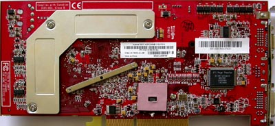 |
| The back side of the card (click for hi-res) |
Underneath the cooler and the metal plate, there is a set of 8 32MB GDD3 memory chips, resulting in the 256MB capacity.

The memory type used is the K4J55323QF-GC20 from Samsung. The speed of 2.0ns which translates to 500MHz, leaves much ground for further overclocking as the stock memory clock frequency only is set to 350MHz.
Removing the HSF from the card unveils the GPU core and the front set of memories.

On the heatsink, the small copper square is where it contacts the GPU while the two rectangular protrusions contact and hence cool, the front side memory modules.

The X800 chipset uncensored. There are two things worth noticing here. Check the following zoomed-in picture:
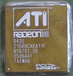
First of all, the label on the core reads "X800 PRO" while this is clearly an X800 vanilla product. Second, at the bottom of the picture you can clearly distinguish "PCI-EXPRESS", even though this is an AGP graphics card.
The fact is that this is the exact same chipset we saw on the X800XL card from Connect3D. Still, the X800XL featured 16 pixel-pipelines whilst this one just 12.
The two GPU's look identical so there's no way we can hardmod the X800 into an X800XL. The 4 missing pipelines seem to be laser-cut as none of the people that tried to flash the vanilla with an XL BIOS managed to unlock them.
The explanation for the PCI-Express logo found on the X800's core, lies beneath the pink covering on the chipset at the back of the card which you can see below:

That chipset is actually the famous RIALTO chipset ATi was preparing some time ago. It translates all PCI signals coming from the card into AGP signals so that the GPU can communicate with the AGP bus interface. This means that ATi no longer has to create two different versions for each of its processors.
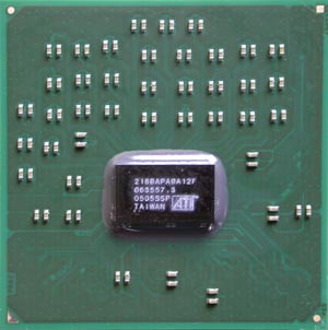 |
| Removing the cover, reveals the rest of circuitry on the RIALTO chipset |
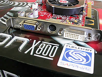
The card's output, as in most cases, consists of one standard VGA for CRT monitors, one DVI-I for TFT monitors and a D-sub for VIVO use.


