Toshiba and SanDisk Start Construction of Fab 5 for NAND Flash Memory
Toshiba today announced that it has started construction of
a fabrication facility (fab), Fab 5, at Yokkaichi
Operations, its memory production facility in Mie
Prefecture, with construction work scheduled for completion
in Spring 2011.
In addition, Toshiba and SanDisk have signed primary
agreements for a new joint venture to operate in the Fab 5
facility.
Construction of the new fab reflects expectations for increasing demand for NAND flash memory for existing and emerging applications, such as smartphones and solid-state drives. Adding new production capacity will ensure that Toshiba and SanDisk are able to respond quickly to market expansion.
The fab building will be constructed in two phases, with the pace of investment reflecting market trends. On completion of its second phase, Fab 5 will be comparable to Fab 4, with a ground area of some 38,000m2. The partners have flexibility as to the extent and timing of their respective fab capacity ramps, and the output allocation will be in accordance with the proportionate level of equipment funding. The initial manufacturing process will be the leading-edge 20-nanometer generation, with subsequent generations to follow.
Fab 5 will have a quake-absorbing structure and is designed to impose minimal environmental impacts. Extensive use of LED lighting throughout the facility, energy-saving manufacturing equipment, and use of inverter-controlled pumps for semiconductor production equipment are expected to cut CO2 emissions to a level 12% lower than for Fab 4.
Yokkaichi Operations currently has four NAND flash memory fabs. Toshiba and SanDisk are currently ramping into the unused clean room space in Fab 4, and expect to reach full capacity of Fab 4 by the start of production in Fab 5.
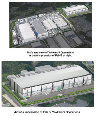
Outline of Fab 5
Structure of building: 2-Story steel frame concrete, five floors
Ground area: Approximately 38,000m2
Total floor area: Approximately 187,000m2
Construction start: July 2010
Completion of first phase: Spring 2011 (Planned)
Outline of Yokkaichi Operations
Location: 800, Yamanoisshiki-cho, Yokkaichi, Mie Prefecture
Established: January 1992
General Manager: Koji Sato
Employees: Approximately 4,300
(as of end of March, 2010, regular employees only for Toshiba)
Site area: Approximately 436,800 m2 (including Fab 5)
Total floor area: Approximately 647,000m2 (including Fab 5)
Construction of the new fab reflects expectations for increasing demand for NAND flash memory for existing and emerging applications, such as smartphones and solid-state drives. Adding new production capacity will ensure that Toshiba and SanDisk are able to respond quickly to market expansion.
The fab building will be constructed in two phases, with the pace of investment reflecting market trends. On completion of its second phase, Fab 5 will be comparable to Fab 4, with a ground area of some 38,000m2. The partners have flexibility as to the extent and timing of their respective fab capacity ramps, and the output allocation will be in accordance with the proportionate level of equipment funding. The initial manufacturing process will be the leading-edge 20-nanometer generation, with subsequent generations to follow.
Fab 5 will have a quake-absorbing structure and is designed to impose minimal environmental impacts. Extensive use of LED lighting throughout the facility, energy-saving manufacturing equipment, and use of inverter-controlled pumps for semiconductor production equipment are expected to cut CO2 emissions to a level 12% lower than for Fab 4.
Yokkaichi Operations currently has four NAND flash memory fabs. Toshiba and SanDisk are currently ramping into the unused clean room space in Fab 4, and expect to reach full capacity of Fab 4 by the start of production in Fab 5.
Outline of Fab 5
Structure of building: 2-Story steel frame concrete, five floors
Ground area: Approximately 38,000m2
Total floor area: Approximately 187,000m2
Construction start: July 2010
Completion of first phase: Spring 2011 (Planned)
Outline of Yokkaichi Operations
Location: 800, Yamanoisshiki-cho, Yokkaichi, Mie Prefecture
Established: January 1992
General Manager: Koji Sato
Employees: Approximately 4,300
(as of end of March, 2010, regular employees only for Toshiba)
Site area: Approximately 436,800 m2 (including Fab 5)
Total floor area: Approximately 647,000m2 (including Fab 5)