Toshiba, SanDisk Mass Produce 15nm NAND flash Memory
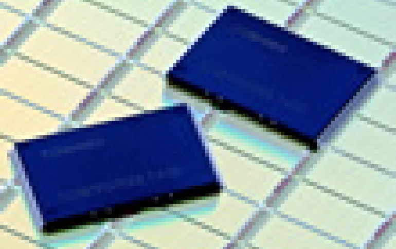
Partners Toshiba and SanDisk have developed 15-nanometer process technology for NAND flash memory used in smartphones and tablets.
The development is the first in the world and will replace the second-generation 19-nm process technology when production begins at Toshiba?s Fab 5 plant in Yokkaichi, Japan, Toshiba said.
The 15-nanometer (nm) process technology which be applied to 2-bit-per-cell 128-gigabit (16 gigabytes) NAND flash memories.
Toshiba and Sandisk have achieved the smallest class chip size with the 15nm process plus improved peripheral circuitry technology. The new chips achieve the same write speed as chips formed with second generation 19 nm process technology, but boost the data transfer rate to 533 megabits a second, 1.3 times faster, by employing a high speed interface.
Toshiba is now applying the 15nm process technology 3-bit-per-cell chips, and aims to start mass production in the first quarter of this fiscal year, to June 2014. The company will develop controllers for embedded NAND flash memory in parallel and introduce 3-bit-per-cell products for smartphones and tablets, and will subsequently extend application to notebook PCs by developing a controller compliant with solid state drives (SSD).
SanDisk will use the new 15nm technology on both two bits-per-cell (X2) and three bits-per-cell (X3) NAND flash memory architectures. The company's All-Bit-Line (ABL) architecture, which contains proprietary programming algorithms and multi-level data storage management schemes, has been implemented in the 1Z technology. SanDisk?s 1Z technology will be utilized across its broad range of solutions, from removable cards to enterprise SSDs.


