Toshiba Starts Construction of Fab 6 at Yokkaichi, Japan
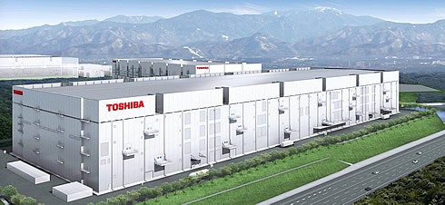
Toshiba has started construction of a new state-of-the-art semiconductor fabrication facility, Fab 6, and a new R&D center, the Memory R&D Center, at Yokkaichi Operations in Mie prefecture, Japan, the company's main memory production base.
Fab 6 will be dedicated to production of BiCS FLASH, Toshiba's 3D Flash memory. Like Fab 5, construction will take place in two phases, allowing the pace of investment to be optimized against market trends, with completion of Phase 1 scheduled for summer 2018. Toshiba will determine installed capacity and output targets and schedules by closely monitoring the market.

Toshiba will also construct a Memory R&D Center adjacent to the new fab, with completion targeting December 2017. The facility will advance development of BiCS FLASH and new memories.
In the meantime, Toshiba has reportedly received bids ranging from 200 billion yen to as much as 400 billion yen ($1.8-3.6 billion) for a 19.9 percent stake in its flash memory business.
The Japanese conglomerate is seeking to raise around 300 billion yen from the sale, according to a Reuters report.
A sale at that price would help Toshiba offset a multi-billion dollar writedown on its U.S. nuclear power business, which investors worry could wipe out shareholder equity.
Suitors for the Japanese company's chip unit include rivals SK Hynix and Micron Technology, Western Digital, Foxconn and financial investors such as Bain Capital.
A Toshiba spokeswoman said the company could not comment on specifics of the sale process.


