H L Data Storage Store Banner 970x90
Breaking News

Seagate releases New Enterprise-Class 5550 /5350 Nytro SSDs SK hynix Develops World’s Highest 238-Layer 4D NAND Flash Samsung Electronics Unveils Far-Reaching, Next-Generation Memory Solutions at Flash Memory Summit 2022 ATP Introduces High-Endurance M.2 2230 SSDs Packed with Customizable Security Features Kioxia Launches Second Generation of High-Performance, Cost-Effective XL-FLASH™ Storage Class Memory Solution

logo

  • Share Us
    • Facebook
    • Twitter
  • Home
  • Home
  • News
  • Reviews
  • Forum
  • Legacy
  • About
    • Submit News

    • Contact Us
    • Privacy

    • Promotion
    • Advertise

    • RSS Feed
    • Site Map

Search form

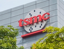
TSMC to Begin Research on 2 nm Chip Manufacturing Nodes

TSMC to Begin Research on 2 nm Chip Manufacturing Nodes

Enterprise & IT Jun 13,2019 0

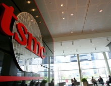
According to taiwanese media, TSMC is expected to build a 2 nanometer (nm) technology factory at its 3 nm facility in Hsinchu, Taiwan.

The company's plan is to complete the 3 nm facility by 2021 and begin 3 nm mass production in 2022. The 2 nm node could become operational two years later. Chinese TechWeb reports that TSMC spokesperson Zhuang Zishou confirmed the 2 nm node facility in Hsinchu.

Meanwhile, two of the world’s largest foundries— TSMC and Samsung announced in April progress in their 5 nm manufaacturing processes. TSMC said its 5 nm manufacturing process is now in what’s called “risk production”. Samsung followed made a similar claim.

TSMC says its 5 nm process offers a 15 percent speed gain or a 30 percent improvement in power efficiency. Samsung is promising a 10 percent performance improvement or a 20 percent efficiency improvement. Obviously, the compared, with the sometimes 50 percent improvements of a decade ago, Moore’s Law is not what it used to be.

The 5 nm node is the first to be built from the start using extreme ultraviolet lithography (EUV). With a wavelength of just 13.5 nm, EUV light can produce extremely fine patterns on silicon. Still, some of these patterns could be made with the previous generation of lithographic tools. This means that those tools would have to lay down three or four different patterns in succession to produce the same result that EUV manages in a single step.

At 5 nm, the foundries are thought to be using 10 to 12 EUV steps, which is alomost the one third of the steps they would require if they could use the older technology.

Before moving to the 5 nm, both Samsung and TSMC foundries are expected to offer a variety of technologies with incremental improvements, in what they’re calling a 6 nm process.

Samsung and TSMC are the only players in the high-end EUV chip making market. GlobalFoundries gave up at 14 nm and Intel, which is years late with its rollout of an equivalent to competitors’ 7 nm, is thought to be pulling back on its foundry services.

Recently, Samsung managed to scoop important deals involving Nvidia’s upcoming Ampere GPUs and Qualcomm’s next gen Snapdragon 865 SoC.

Tags: TSMCSamsung foundry2nm5nm
Previous Post
VW Ford Deal on Autonomous and Electric Cars Close to Finalization
Next Post
Shinano Kenshi Introduces New ASPINA Corporate Brand

Related Posts

  • TSMC to boost 5nm chip output in 2H21

  • ASML Ships Multibeam Inspection System ‘eScan1000’ For Advanced Technology Nodes

  • TSMC Announces 7nm Automotive Design Enablement Platform

  • Samsung Expands its Foundry Capacity with A New 5nm Chip Production Line in Pyeongtaek, Korea

  • Synopsys and TSMC Collaborate to Enable Designs of HPC, Mobile, 5G, and AI SoCs with Certified Solutions on TSMC N5 and N6 Processes

  • TSMC Does Not Accept New Orders From Huawei: Nikkei

  • TSMC to Build Arizona Chip Plant

  • Trump In Talks With Chip Makers Including TSMC to Bring Factories in the US: report

H L Data Storage Store Banner 300x600


Latest News

Seagate releases New Enterprise-Class 5550 /5350 Nytro SSDs
Enterprise & IT

Seagate releases New Enterprise-Class 5550 /5350 Nytro SSDs

SK hynix Develops World’s Highest 238-Layer 4D NAND Flash
Enterprise & IT

SK hynix Develops World’s Highest 238-Layer 4D NAND Flash

Samsung Electronics Unveils Far-Reaching, Next-Generation Memory Solutions at Flash Memory Summit 2022
Enterprise & IT

Samsung Electronics Unveils Far-Reaching, Next-Generation Memory Solutions at Flash Memory Summit 2022

ATP Introduces High-Endurance M.2 2230 SSDs Packed with Customizable Security Features
Enterprise & IT

ATP Introduces High-Endurance M.2 2230 SSDs Packed with Customizable Security Features

Kioxia Launches Second Generation of High-Performance, Cost-Effective XL-FLASH™ Storage Class Memory Solution
Enterprise & IT

Kioxia Launches Second Generation of High-Performance, Cost-Effective XL-FLASH™ Storage Class Memory Solution

Popular Reviews

CeBIT 2005

CeBIT 2005

CeBIT 2006

CeBIT 2006

Zidoo Z9S 4K Media Player review

Zidoo Z9S 4K Media Player review

LiteOn iHBS112 review

LiteOn iHBS112 review

Club3D HD3850

Club3D HD3850

External USB Slim Recorders Comparison

External USB Slim Recorders Comparison

Pioneer BDR-2207 (BDR-207M) BDXL burner review

Pioneer BDR-2207 (BDR-207M) BDXL burner review

Crucial P1 NVMe 1TB SSD review

Crucial P1 NVMe 1TB SSD review

  • Home
  • News
  • Reviews
  • Forum
  • Legacy
  • About
    • Submit News

    • Contact Us
    • Privacy

    • Promotion
    • Advertise

    • RSS Feed
    • Site Map
  • About
  • Privacy
  • Contact Us
  • Promotional Opportunities @ CdrInfo.com
  • Advertise on out site
  • Submit your News to our site
  • RSS Feed