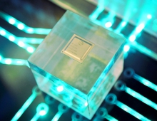
An Update on TSMC's Processes and Roadmap
Last week was TSMC's Open Innovation Platform Innovation Forum (OIP) and the company provided an update of its current chip production plans.
TSMC's Cliff Hou said that the N5 (5nm) manufacturing perocess is ready, with risk production started in March. This proposition is optimized for both mobile and HPC. It will be followed by N5P (P for performance) with risk production starting a year after N5, so that would be about March 2020.
Comparing N5 to N7, it is 15% faster, 30% lower power, according to TSMC. Of course, this means that you can get a speed increase of 15% at the same power, or a power reduction of 30% at the same performance. It does not mean you can get both at the same time. Obviously, you can also blend the two and take a part of the improved process as a performance increase and a part as power reduction. TSMC also said that N5's logic density is 1.8X, SRAM scaling is 0.75, analog scaling around 0.85.
The N5 is that it is fully-fledged EUV adoption, which reduces cycle time due to fewer steps that multi-pattern everything. It is enhanced with a transistor with a high-mobility channel for both performance and power. There are other architectural features that enable logic and SRAM density scaling. There are low-resistance contacts and vias. The I/O transistor can be either 1.5V or 1.2V.
N5 HPC has extreme Vt LVT device that is 25% faster than N7. The HPC standard-cell library has optimized metal and a via pillar array to further boost performance by 10%. There is a special device offering to enable 112Gbps SerDes. For decap capacitors, there is a super high desngith MIM (SHDMIK) that provides 4X more decap than HDMIM (MIM stands for metal-insulator-metal, since these capacitors are built in the BEOL in the metal stack). The increase in decap results in an extra 4% speed boost at the same voltage.
For analog, TSMC have taken a new approach with N5 Restricted Design Rules (RDR). They have provided an analog cell library that goes beyond just providing transistors in the PDK. This improves the manufacturing window. The analog cells are transistors in abuttable layout templates with predefined cell-heights and pre-drawn layout patterns for the m0 layer and below. Each transistor is surrounded by predefined and validate technology. It achieves much better SPICE to silicon correlation than the non-RDR approach. To build an analog block, you build the schematic using these cells instead of transistors, then route the metal layers on top after placement. Finally, add the guard-ring and boundary cells for a final DRC-clean design.
The N7, compared to 16FF+ is 30% faster, 55% reduction in power, 3.3X increase in logic density, 0.38X SRAM area. Mass production started in April 2018. All IP is available.
The N6 is a die cost reduction from N7 by increased use of EUV to reduce process complexity, and improve logic density by 18%, making use of CPODE (continuous poly on diffusion edge). Risk production starts in Q1 2020. There is a yield improvement from the smaller die size and the reduction in layers.
Cliff also talked about packaging. TSMC has two basic technologies called InFO (integrated fanout) and CoWoS (chip on wafer on substrate).
CoWoS is targeted at very large designs. Currently they can do designs 1.5X the reticle size, in 2020 that will go to 2X and in 2021 to 3X reticle size.
They can do wafer on wafer (WoW) and chip on wafer (CoW). Obviously WoW requires the die size to be identical and the yield to be very high. For CoW they can only use known good die (KGD) that have already been tested.
There is a whole 3D-IC design flow to stack die during verification, perform IR/EM analysis, thermal, signal and power integrity, and more.
On the day of OIP, TSMC had announced a 4GHz CoWoS HPC chiplet-based design, proven in silicon, around an Arm Cortex-A72 and using low-swing 0.3V I/O design that achieved 8Gb/s per pin, giving a total of 320GB/s.