Samsung Develops World's Smallest DRAM Technology
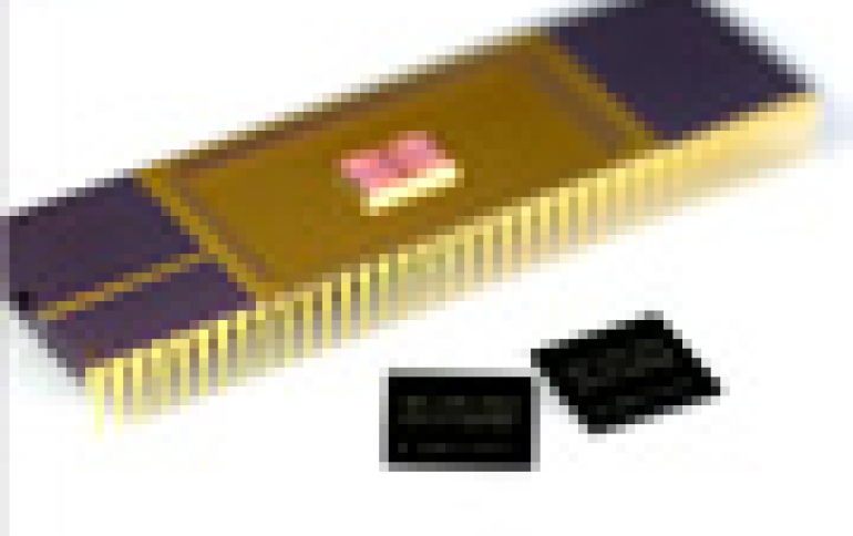
Samsung Electronics claims it has developed a 512-Mb DDR2 SDRAM memory chip with 70-nanometer processing technology - a sort of grand slam in miniaturizing DRAM technology.
The new technology will yield at least twice as many chips from a single wafer
than the 90 nm processing technology, and chips will work at an energy-saving
1.8 volt. In addition, the manufacturing breakthrough has been achieved using
Samsung's Metal-Insulator-Metal capacitor technology, and 3D transistor
architecture known as 'Sphere-shaped Recess Channel Array Transistor'. These
technologies have been applied to overcome the limitations of stacked DRam
cells and improve the data refresh function, critical to the 70nm 512Mb DRam.
Samsung says it will show the best performance not only in computers but especially in mobile devices, where size matters most. After the 90 nm technology currently in use in mass production and the 80 nm technology, Samsung Electronics will start applying the new 70 nm technology from second half of next year.
The unveiling of a 70nm DRam fabrication process follows on from Samsung's development of the first sub-micron DRAM process in 2002 and 80nm memory processing in 2003.
The firm said that its 70nm process technology is scheduled to be used in production in the second half of 2006 for 512Mb, 1Gb and 2Gb densities.
The global DRAM market is expected to grow from US$26.5 billion this year to S$37.4 billion by 2009, largely due to the release of next-generation game consoles, third-generation mobile phones and the launch of the new Microsoft operating system Vista.


