Toshiba Starts Sampling 64-Layer, 512-gigabit 3D Flash Memory
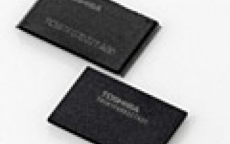
Toshiba has today unveiled the latest addition in its line-up of BiCS FLASH three-dimensional flash memory with a stacked cell structure, a 64-layer device that achieves a 512-gigabit (64-gigabytes) capacity with 3-bit-per-cell (triple-level cell, TLC) technology.
The new device will be used in applications that include enterprise and consumer SSD. Sample shipments of the chip started this month, and mass production is scheduled for the second half of this calendar year.
Toshiba continues to refine BiCS FLASH, and the next milestone on its development roadmap is the industry's largest capacity, a 1-terabyte product with a 16-die stacked architecture in a single package. Plans call for the start of sample shipments in April 2017.
For the new 512-gigabit device, Toshiba deployed 64-layer stacking process to realize a 65% larger capacity per unit chip size than the 48-layer 256-gigabit (32-gigabytes) device, and has increased memory capacity per silicon wafer, reducing the cost per bit.
Toshiba's Memory business already mass produces 64-layer 256-gigabit (32-gigabytes) devices and will expand BiCS FLASH production.
Toshiba hopes it will be able sell its memory chip division and survive the crisis caused by a writedown at its nuclear business.
This week, the Tokyo-based company completed the sale of its medical finance unit. Media reports said a buyer of its prized flash memory business could be chosen in May, and the world's biggest contract maker of chips could be a bidder. The company is said to be looking to raise at least 1 trillion yen ($8.8 billion) from the sale of its memory chip unit as it grapples with a $6.3 billion writedown at its nuclear division.
Taiwan Semiconductor Manufacturing Co., the biggest contract maker of chips, may aim to boost cooperation with Toshiba by investing in its memory business, the Nikkan Kogyo newspaper reported Wednesday.


