TSMC is Mass Producing EUV-based N7+ Technology
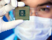
TSMC's seven-nanometer plus (N7+), the industry’s first commercially available Extreme Ultraviolet (EUV) lithography technology, is delivering products to market in high volume.
The N7+ process with EUV technology is built on TSMC’s 7nm node and paves the way for 6nm and more advanced technologies.
TSMC says that N7+, which began volume production in the second quarter of 2019, is matching yields similar to the original N7 process that has been in volume production for more than one year.
N7+ is also providing improved overall performance. When compared to the N7 process, N7+ provides 15% to 20% more density and improved power consumption, ccording to TSMC. The company says it has been quickly deployed capacity to meet N7+ demand that is being driven by its multiple customers.
EUV technology enables TSMC to keep driving chip scaling as the shorter wavelength of EUV light is better able to print the nanometer-scale features of advanced technology designs. TSMC sayys that its EUV tools have reached production maturity, with tool availability reaching target goals for high-volume production, and output power of greater than 250 watts for day-to-day operations.
TSMC also plans to bring N6 technology into risk production in the first quarter of 2020 for volume production by the end of the year. With further application of EUV, N6 is expected to offer 18% higher logic density over N7, and design rules fully compatible with N7 enable TSMC's customers to shorten time-to-market.

