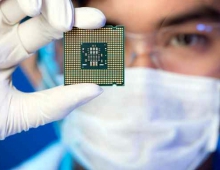
Samsung Outlines Possible Solutions For EUV Process Challenges
Despite tremendous progress in the EUV (Extreme Ultraviolet) process technology used in the microfabrication process of semiconductor, several challenges still need to be tackled. Samsung Electronics presented various solutions such as extreme low-temperature process and extreme low-pressure process to resolve some ot these challenges.
During ‘The Korean Society of Semiconductor & Display Technology Fall Conference’ held at the Hanyang University on November 19th, Samsung Electronics' Master Park Jong-cheol said that there are currently two obstacles in the etching process that removes circuits as the semiconductor industry is starting move into the EUV process era.
The firet issue is the so-called ‘micro bridge’ random failures that occur at the bottom of a circuit. In addition, it has become difficult to place a material deep inside in order to pill off circuits as the width of the circuits has become extremely narrow.
EUV process is a photolithography process that repeatedly prints circuits on a circular wafer using an EUV light source (13.5nm). Since the wavelength is about 14 times smaller than the wavelength of ArF (Argon Fluoride, 193nm), the most commonly used light source, the EUV process can print more accurate circuits.
However, this shorter wavelength causes new flaws such as micro bridge.
During the during photolithography process, a EUV photoresist is applied on a semiconductor wafer. The main issue here is that the energy of the wavelength of EUV light source becomes 10 times greater as the wavelength becomes shower. Because the wavelength and the energy are inversely proportional, the wavelength hits the surface of a wafer harder as it becomes shorter. The high energy light source either causes the nucleus of an atom of a reactant to either pop out from the EUV photoresistor or pushes new atoms to combine. The result is the unwanted formation of foreign substances. In addition, the width of a circuit become thinner causing areas that are not supposed to be pilled off to be connected.
“Although photolithography process can be lengthened in order to resolve micro bridge issue, we have to consider the fact that the productivity of an EUV photolithography system that costs about $171 million (200 billion KRW) can decline faster.” said Master Park.
He said that Samsung has chosen a method that repeatedly shaves off micro bridges while protecting the upper part of a circuit with polymer.
“Because it may be difficult to maintain this method for next-generation processes, it is likely that we are going to need a brand new etching technology.” said Master Park.
Another problem is that it has become more difficult to place materials that are needed for etching process deep inside a circuit, since the width of the circuit has become significantly narrower. Polymers cover the surface during the etching process in order to prevent circuits from shaved off unevenly.
The problem is that circuits made through EUV are already thin and that the polymer currently used makes the entrance even narrower, causing a ‘bottleneck phenomenon’. As a result, more time and costs are required in order to place etching materials and ions deep inside through a narrow entrance.
Master Park suggested that using an ‘extreme low-temperature’ etching process as a possible solution. By decreasing the temperature inside of a chamber where wafers are placed, gaseous movements that are necessary for the etching process are minimized even without a polymer. His solution is based on a principle that materials that are active in room temperature move slowly in extreme low-temperatures.
“Extreme low-temperature method to create effective etching materials and ‘high pumping’ etching technology that prevents bottleneck phenomenon by forcing gas inside of a chamber to move faster can be possible alternatives.” said Master Park. “Samsung Electronics is currently conducting R&D on these technologies to apply them to actual mass-production process.”